Making Things
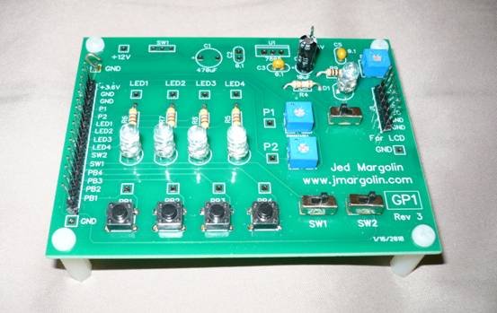
Project GP1 - Board for demonstrating how to use an MSP430G2xxx. The board has four pushbutton switches, four LEDs, two slide switches, two trimpots, +5V regulator for the LCD, trimpot for the LCD, and backlight switch for the LCD. I designed it to be used with the original MSP-EXP430G2 LaunchPad. TI says that it is now obsolete and to use the new MSP-EXP430G2ET Launchpad. http://www.ti.com/tool/msp-exp430g2et . TI says you can order the new MSP-EXP430G2ET directly from them for $9.99. Here is the MSP-EXP430G2ET User Guide slau772: Click here.
This new Launchpad is a little different. It runs on 3.3V instead of 3.6V but it also provides +5V which the original Launchpad did not. As a result the external power supply for providing +5V for an LCD display is no longer needed. To use it with the new Launchpad leave out SW1, C1, C2, and U1 (7805 regulator) and connect the +5V test point to the Launchpad 5V pin. If the 5V is low remember that it is coming from the computer’s USB port.
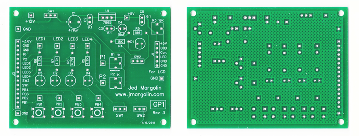
For the schematic of the GP1 click here.
The GP1 board supports a 16x2 LCD at header J1 with +5V and the contrast control. The data will come directly from the Launchpad. Switch SW2 switches a 100 Ohm resistor in or out of the current going to the LED backlight. The data must come from the Launchpad. Although the 16x2 LCD panels are available in lower voltage versions I use the standard 5V version. For the datasheet click here. These LCD panels use a Hitachi HD44780 controller. For the datasheet click here. When operated at between 4.5 and 5.5V the HD44780 takes everything above 2.2V as a logic high (PDF page 51). That means you can use it with a 3.3V device without a level translator but you must only write to it. The datasheet does not specify what a logic ‘1’ output is but since it runs on 5V it could be 5V. You have heard of a Read-Only Memory. Well, consider this a Write-Only Memory. It works fine with fixed write timing. The datasheet shows all of the fonts and how to define your own characters.
The components on the board connect to the Launchpad through header J3.
I use male headers and connect to the Launchpad with female to female jumper wires. On eBay the headers are called 2.54mm Male PCB Single Row Straight Header Strip Connector Arduino.
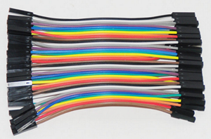
The jumper wires are called 40 Wire Female to Female Jumper Wire for Arduino. They come in various lengths.
If the LEDs are too bright increase the values of the series resistors.
And now the software.
I use Texas Instruments Code Composer Studio. It’s free and it works fairly well although it is not easy to come up to speed on it. It works really well with TI’s Launchpad. I will assume that you already know how to use CCS or you can figure it out. You can get it here: http://www.ti.com/tool/CCSTUDIO.
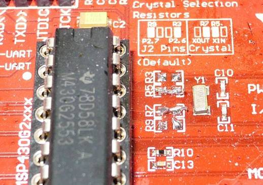
The original MSP430G2 LaunchPad came with a 32.768 KHz crystal that you had to solder onto the board if you wanted to use it. The new MSP-EXP430G2ET comes with the crystal on the board but:
By default, the crystal is not connected to the MSP430G2553 because the target pins are multiplexed with two BoosterPack plug-in module header pins. 0-Ω resistors R3 and R9 must be removed, while R5 and R7 must be shorted across to connect the external crystal to the MSP430G2553. See the onboard crystal selection resistors silkscreen for how to configure the resistors to select between the crystal or the BoosterPack plug-in module pins.
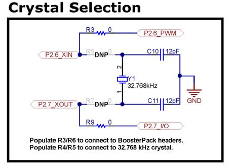
Ok, that should be easy but I see a problem here. The crystal and the oscillator need the two capacitors (C10 and C11) in order to work properly. The MSP430G2xxx has internal capacitors that can be selected in the software so you don’t need external capacitors. The new Launchpad has the capacitors stuffed. The old Launchpad has pads for SMD capacitors (C21 and C22) but does not come with them. So a program for the old Launchpad (and your circuit) would use the internal capacitors but a program for the new Launchpad would not. If this is a problem you can do one of the following:
1. Remove C10 and C11 from the new Launchpad and use the internal capacitors. This way you can use either the new Launchpad or the old one interchangeably.
2. Add a Conditional Compile to the software so that you use the external capacitors when using the new Launchpad but the internal capacitors when using the old Launchpad or when using your circuit. This assumes your circuit does not use external capacitors.
3. Add C21 and C22 to the old Launchpad and to your circuit.
4. Use only the new Launchpad and have the capacitors on your board.
5. Do your code to use the internal capacitors and see if it works with the new Launchpad anyway.
Oh, and remove jumpers P1.0 and P1.6 on the Launchpad in order for it to work with your hardware because some of the target I/O pins go to LEDs and pushbuttons in order to run their demo software. See PDF page 25 of the manual SLAU772 above. Be careful not to lose the little black shorting caps. When I remove one I put it back on just one of the pins so it hangs over the side.
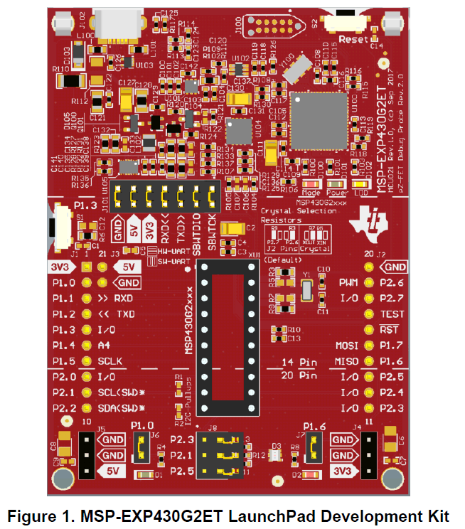
Here is the picture of the MSP-EXP430G2ET from TI’s manual:
Here I have zoomed in on the oscillator section.
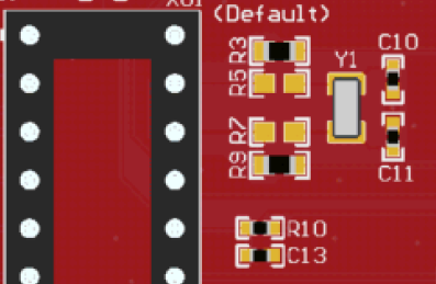
I removed R3 and R9 and shorted the pads for R5 and R7 respectively.
Ok, I am not great at doing SMT by hand.
Once you become familiar with the MSP430G2xxx family you should buy more of the parts you want to use. You can buy them from Newark, Digikey, Mouser, and other places. They all seem to charge the same except that sometimes Newark (www.newark.com) has special deals. They change from time to time. As I write this in May 2019 they are selling the MSP430G2302IN20 for $0.55 (any quantity). The MSP430G2302 is pretty decent. It has 4 KBytes of Flash, 256 bytes of RAM, and an SPI interface but it doesn’t have the 10-Bit Analog-to-Digital (A/D) converter. If you don’t need the ADC the MSP430G2302 is a good choice.
Now about running CCS. When I write a new program I start with code I have already written. There are some things that most of my programs use, like initializing the ports, initializing the clock to 16MHz using the 32.758 KHz crystal, and interrupts which I sometimes use.
I am not an expert. The following is how I get code into it, build it, and run it.
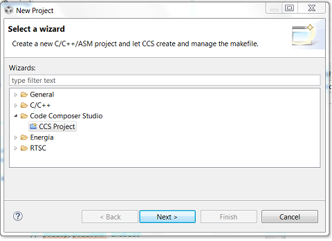
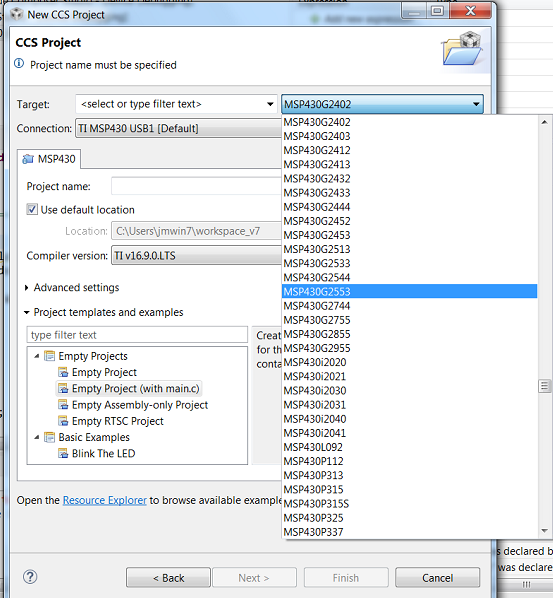
1. Start a new project.
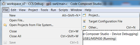
2. Select CCS Project
The first thing to do is select which processor to use.
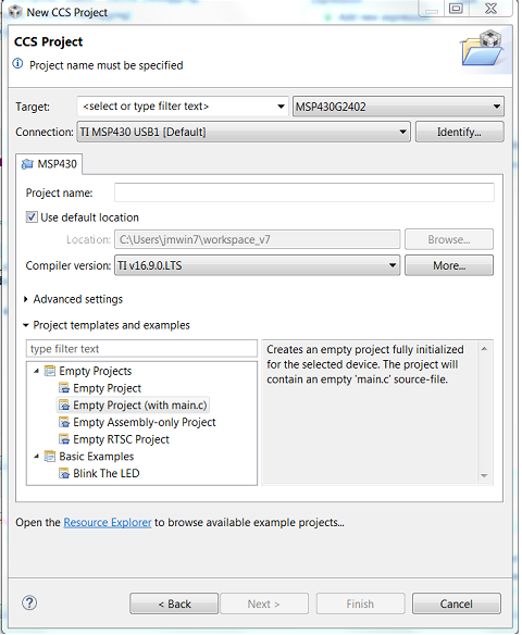
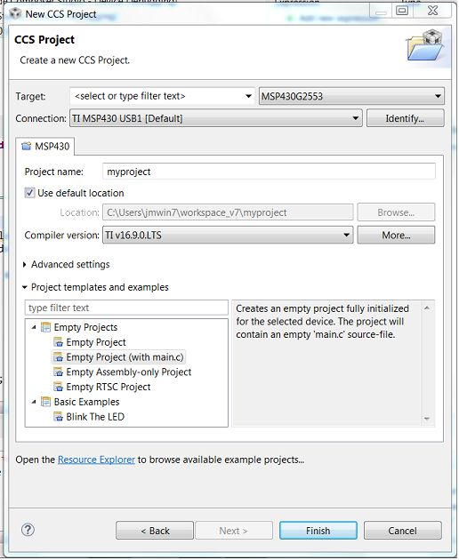
We will be using the MSP430G2553 so it will be usable by all of the programs here and because the Launchpad comes with a MSP430G2553.
Now choose a name for the project and under Project Templates and examples make it an Empty Project (with main.c)
It will create main.c with this code:
|
#include <msp430.h>
/* * main.c */ int main(void) { WDTCTL = WDTPW | WDTHOLD; // Stop watchdog timer return 0; }
|
Now delete that code and open the program that you want with NotePad or WordPad, such as gp1-led-main.c.txt .
Select All and Copy.
Go back to main.c and Paste.
Now my code (or your code) is in main.c
If you want to start with an existing CCS main.c program from another project then open it, Select All, and Copy that code into the new main.c .
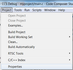
If you want to change the processor go to Project Properties.
Select General and then select the processor you want to use.
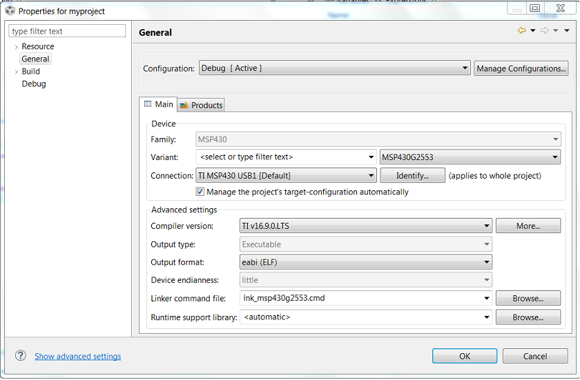
There is one more thing you should do here even if you are not changing processors. Select Build Optimization.
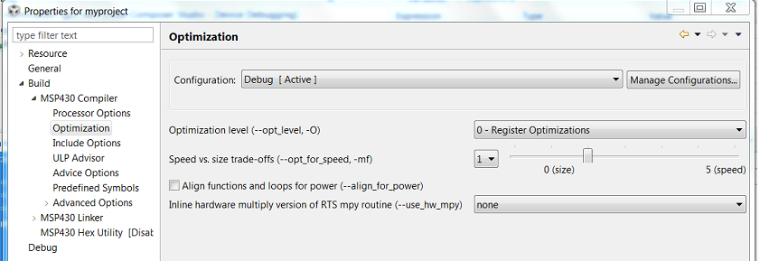
Select 0 - Register Optimizations. Otherwise it will tend to remove my software timing code.
It has the mindset that if you want to time something you should do it with interrupts so the processor can go to sleep between interrupts to save power.
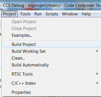
Then build the project.
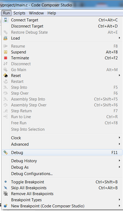
Run Debug. It should download the code.
And Go Main.
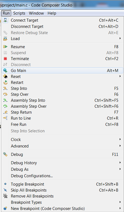
If the code was downloaded into the Launchpad and everything else has gone right that should run the program.
Code For Project GP1:
Program 1 - Controls the LEDs. Displays a 4-bit binary counter.
Program 2 - Pushbutton switches control the corresponding LEDs. Switch is pressed the LED is on. Switch is released the LED is off.
Program 3 - Debounce the switches and toggle the respective LEDs
Program 4 - Debounce pb1. When pb1 is pressed, roll the LEDs.
Program 5 - This shows why you need to debounce switches.
Program 6 - Demonstrate the 16x2 LCD including hex to BCD conversion
Program 7 - Reads Pot 1 and Pot 2 with the ADC (12-bit) and displays the hex values on the LCD.
Program 8 - Reads Pot 1 and Pot 2 with the ADC (12-bit) and displays the hex values on the LCD. Does some simple filtering.
First, some software topics.
1. Debouncing switches - When mechanical switches close, their contacts bounce for a short amount of time. It also happens when the switch contacts open. If this is not dealt with properly the switch can trigger multiple (and undesired) events.
One method is to use an SPDT switch with an RS Flip-Flop.
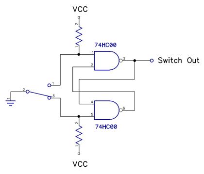
The switch is more expensive and it uses more wires and more parts.
Another method is to use an RC filter with a gate with a Schmitt trigger input.
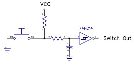
The circuit can be slow to operate and it uses more parts. But I use something like this as a reset switch for the MSP430G2xxx whose Reset input has a Schmitt Trigger input. (It’s ok for Reset to be a little slow.)
The following method was developed by the legendary Mike Albaugh of Atari Coin-Op (Atari/Atari Games). Mike made sure that every game had the proper switch debounce code for the player switches and coin switches. (If the coin switches hadn’t been properly debounced, the players would have gotten multiple unmerited credits which would have made the Operators unhappy.) Mike also provided the coin routines which could be complicated because of all the options that the Operators needed to be able chose. He also did a great many other things. I wish he would write about his many years at Atari/Atari Games.
The switch circuit is very simple.
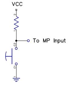
The debouncing is done in software.
A memory byte is dedicated to each switch. Let’s call it swstate which is initialized to all ones (0xFF).
|
1 |
1 |
1 |
1 |
1 |
1 |
1 |
1 |
Periodically the state of the switch is shifted into swstate.
When swstate is all zeros (0x00) the switch is closed, which is easy to test for.
|
0 |
0 |
0 |
0 |
0 |
0 |
0 |
0 |
When swstate is all ones (0xFF) the switch is open, which is also easy test for.
|
1 |
1 |
1 |
1 |
1 |
1 |
1 |
1 |
While the switch is bouncing, swstate will contain a mix of ones and zeros such as:
|
1 |
0 |
0 |
1 |
1 |
0 |
0 |
1 |
This is also easy to test for because it will fail the all ones and all zeros tests.
Mike read the switches four times during the NTSC video frame which comes out to about every 4 ms. Mike’s method was very reliable regardless of the type of switch and was used in all of our games. It was so good that the other game companies copied it, thereby making it an industry standard.
2. Converting hex to BCD
The conventional method of converting hex to BCD requires several divisions and multiplications. That is too slow so I am using the method I vaguely remembered from my days at Atari called the Shift-and-Add method. Basically, as you divide the hex number by two (a shift) you multiply the BCD result by two by adding it to itself using a decimal addition. I didn’t quite remember how our Programmers did it. I know the 6502 has a decimal mode that makes the ADD (and ADC) instructions do a decimal addition of two packed BCD numbers. When I did it here (in C) I used the principle that if the result of adding two nybbles is greater than 9 (like 12, which is 0x0B in hex and not a BCD number) then I subtract 10 and get 2 and set a half-carry flag which will be added to the next nybble. For example, if I start with a packed BCD number containing 0x06. I add it to itself to get 0x0B which is decimal 12. I subtract 10 (0x0A) and get 0x02 (decimal 2). The half carry is set so that a 0x01 will be added to the next nybble to make it 0x12 which is the correct packed BCD number. BCD is confusing because we are representing a decimal number in hex (actually binary). I started writing the code and hacked away at it until it produced the correct results. (I’m an Engineer, not a Programmer.) There are probably faster ways of doing this especially if you do it in MSP430G2xxx assembly code since the processor has DADD (decimal add) and DADC (decimal add with Carry) instructions. For the MSP430G2xxx Instruction Set Summary click here.
Here is my code.
Program 1: gp1-led-main.c.txt
Controls the LEDs. Displays a 4-bit binary counter.
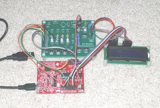
Here is how to connect the GP1 to the Launchpad.
|
Launchpad |
Pin |
|
GP1 |
|
Ground |
20 |
|
GND |
|
P1.4 |
6 |
|
LED1 |
|
P1.5 |
7 |
|
LED2 |
|
P1.6 |
14 |
|
LED3 |
|
P1.7 |
15 |
|
LED4 |
Program 2: gp1-sw1-main.c.txt
Pushbutton switches control the corresponding LEDs. When the switch is pressed the LED is on. When the switch is released the LED is off.
|
Launchpad |
Pin |
|
GP1 - J3 |
Alternative |
|
Ground |
20 |
|
GND |
GND |
|
P1.0 |
2 |
|
PB1 |
SW1 (Slide Switch |
|
P1.1 |
3 |
|
PB2 |
SW2 (Slide Switch) |
|
P1.2 |
4 |
|
PB3 |
PB3 |
|
P1.3 |
5 |
|
PB4 |
PB4 |
|
P1.4 |
6 |
|
LED1 |
LED1 |
|
P1.5 |
7 |
|
LED2 |
LED2 |
|
P1.6 |
14 |
|
LED3 |
LED3 |
|
P1.7 |
15 |
|
LED4 |
LED4 |
Program 3: gp1-sw2-main.c.txt
Debounce the switches and toggle the respective LEDs
|
Launchpad |
Pin |
|
GP1 - J3 |
Alternative |
|
Ground |
20 |
|
GND |
GND |
|
P1.0 |
2 |
|
PB1 |
SW1 (Slide Switch |
|
P1.1 |
3 |
|
PB2 |
SW2 (Slide Switch) |
|
P1.2 |
4 |
|
PB3 |
PB3 |
|
P1.3 |
5 |
|
PB4 |
PB4 |
|
P1.4 |
6 |
|
LED1 |
LED1 |
|
P1.5 |
7 |
|
LED2 |
LED2 |
|
P1.6 |
14 |
|
LED3 |
LED3 |
|
P1.7 |
15 |
|
LED4 |
LED4 |
Program 4: gp1-sw3-main.c.txt
Debounce pb1. When pb1 is pressed, roll the LEDs.
|
Launchpad |
Pin |
|
GP1 - J3 |
Alternative |
|
Ground |
20 |
|
GND |
GND |
|
P1.0 |
2 |
|
PB1 |
SW1 (Slide Switch |
|
P1.1 |
3 |
|
PB2 |
SW2 (Slide Switch) |
|
P1.2 |
4 |
|
PB3 |
PB3 |
|
P1.3 |
5 |
|
PB4 |
PB4 |
|
P1.4 |
6 |
|
LED1 |
LED1 |
|
P1.5 |
7 |
|
LED2 |
LED2 |
|
P1.6 |
14 |
|
LED3 |
LED3 |
|
P1.7 |
15 |
|
LED4 |
LED4 |
Program 5: gp1-sw4-main.c.txt
This shows why you need to debounce switches.
No interrupts, No debouncing at all.
When pb1 is pressed, roll the LEDs
|
Launchpad |
Pin |
|
GP1 - J3 |
Alternative |
|
Ground |
20 |
|
GND |
GND |
|
P1.0 |
2 |
|
PB1 |
SW1 (Slide Switch |
|
P1.1 |
3 |
|
PB2 |
SW2 (Slide Switch) |
|
P1.2 |
4 |
|
PB3 |
PB3 |
|
P1.3 |
5 |
|
PB4 |
PB4 |
|
P1.4 |
6 |
|
LED1 |
LED1 |
|
P1.5 |
7 |
|
LED2 |
LED2 |
|
P1.6 |
14 |
|
LED3 |
LED3 |
|
P1.7 |
15 |
|
LED4 |
LED4 |
Program 6: gp1-lcd-main.c.txt
Demonstrate the 16x2 LCD including hex to BCD conversion
If you are using the old MSP-EXP430G2 LaunchPad stuff SW1, C1, C2, and U1 (7805 regulator) and apply +12V to the board. If you are using the new MSP-EXP430G2ET leave them off and connect the +5V testpad to one of the Launchpad 5V pins.
Uses LCD in 4-bit data mode.
Write a message to the LCD.
Converts a hex byte to BCD (3 digits) and displays it on the LCD.
Converts a hex word to BCD (5 digits) and displays it on the LCD.
Debounce PB1 and control LED1.
For the datasheet for 16x2 LCD panel click here.
These LCD panels use a Hitachi HD44780 controller. For the datasheet click here.
For connecting ground between boards use the 10cm jumpers.
If it comes up and you don’t see anything on the LCD try adjusting the Contrast control (R3).
You don’t have to connect PB2, PB3, PB4, LED3, and LED4 but if they are already connected you can leave them connected.
|
Launchpad |
Pin |
|
GP1 - J3 |
|
Ground |
20 |
|
GND |
|
P1.0 |
2 |
|
PB1 |
|
P1.1 |
3 |
|
PB2 |
|
P1.2 |
4 |
|
PB3 |
|
P1.3 |
5 |
|
PB4 |
|
P1.4 |
6 |
|
LED1 |
|
P1.5 |
7 |
|
LED2 |
|
P1.6 |
14 |
|
LED3 |
|
P1.7 |
15 |
|
LED4 |
|
LCD |
Pin |
|
Launchpad |
Pin |
|
RS |
4 |
|
P2.5 |
13 |
|
E |
6 |
|
P2.4 |
12 |
|
D4 |
11 |
|
P2.0 |
8 |
|
D5 |
12 |
|
P2.1 |
9 |
|
D6 |
13 |
|
P2.2 |
10 |
|
D7 |
14 |
|
P2.3 |
11 |
|
LCD |
Pin |
|
GP1 - J1 |
|
GND |
1 |
|
GND |
|
+5V |
2 |
|
+5V |
|
VO |
3 |
|
Con. |
|
RW |
5 |
|
GND |
|
A |
15 |
|
LED |
|
K |
16 |
|
GND |
To make it a little easier you can print out a PDF of the connections: click here.
And here is what you get.
Program 7: gp1-adc1-main.c.txt
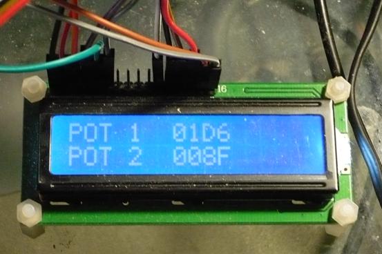
Reads Pot 1 and Pot 2 with the ADC (12-bit) and displays the hex values on the LCD.
If you are using the old MSP-EXP430G2 LaunchPad stuff SW1, C1, C2, and U1 (7805 regulator) and apply +12V to the board. If you are using the new MSP-EXP430G2ET leave them off and connect the +5V testpad to one of the Launchpad 5V pins.
Requires that 3.3V/3.6V be connected to VCC on the Launchpad. It is needed by the pots.
Uses LCD in 4-bit data mode.
For the datasheet for 16x2 LCD panel click here.
These LCD panels use a Hitachi HD44780 controller. For the datasheet click here.
For connecting ground between boards use the 10cm jumpers.
If it comes up and you don’t see anything on the LCD try adjusting the Contrast control (R3).
Pot 1 is read by P1.0 and Pot 2 is read by P1.1 so disconnect them from the switches.
You don’t have to connect PB3, PB4, LED1, LED2, LED3, and LED4 but if they are already connected you can leave them connected.
|
Launchpad |
Pin |
|
GP1 - J3 |
|
Ground |
20 |
|
GND |
|
P1.0 |
2 |
|
Pot1 |
|
P1.1 |
3 |
|
Pot2 |
|
VCC |
1 |
|
3.6V |
|
LCD |
Pin |
|
Launchpad |
Pin |
|
RS |
4 |
|
P2.5 |
13 |
|
E |
6 |
|
P2.4 |
12 |
|
D4 |
11 |
|
P2.0 |
8 |
|
D5 |
12 |
|
P2.1 |
9 |
|
D6 |
13 |
|
P2.2 |
10 |
|
D7 |
14 |
|
P2.3 |
11 |
|
LCD |
Pin |
|
GP1 - J1 |
|
GND |
1 |
|
GND |
|
+5V |
2 |
|
+5V |
|
VO |
3 |
|
Con. |
|
RW |
5 |
|
GND |
|
A |
15 |
|
LED |
|
K |
16 |
|
GND |
Program 8: gp1-adc2-main.c.txt
Reads Pot 1 and Pot 2 with the ADC (12-bit) and displays the hex values on the LCD. Does some simple filtering.
If you are using the old MSP-EXP430G2 LaunchPad stuff SW1, C1, C2, and U1 (7805 regulator) and apply +12V to the board. If you are using the new MSP-EXP430G2ET leave them off and connect the +5V testpad to one of the Launchpad 5V pins.
Requires that 3.3V/3.6V be connected to VCC on the Launchpad. It is needed by the pots.
Uses LCD in 4-bit data mode.
For the datasheet for 16x2 LCD panel click here.
These LCD panels use a Hitachi HD44780 controller. For the datasheet click here.
For connecting ground between boards use the 10cm jumpers.
If it comes up and you don’t see anything on the LCD try adjusting the Contrast control (R3).
Pot 1 is read by P1.0 and Pot 2 is read by P1.1 so disconnect them from the switches.
You don’t have to connect PB3, PB4, LED1, LED2, LED3, and LED4 but if they are already connected you can leave them connected.
|
Launchpad |
Pin |
|
GP1 - J3 |
|
Ground |
20 |
|
GND |
|
P1.0 |
2 |
|
Pot1 |
|
P1.1 |
3 |
|
Pot2 |
|
VCC |
1 |
|
3.6V |
|
LCD |
Pin |
|
Launchpad |
Pin |
|
RS |
4 |
|
P2.5 |
13 |
|
E |
6 |
|
P2.4 |
12 |
|
D4 |
11 |
|
P2.0 |
8 |
|
D5 |
12 |
|
P2.1 |
9 |
|
D6 |
13 |
|
P2.2 |
10 |
|
D7 |
14 |
|
P2.3 |
11 |
|
LCD |
Pin |
|
GP1 - J1 |
|
GND |
1 |
|
GND |
|
+5V |
2 |
|
+5V |
|
VO |
3 |
|
Con. |
|
RW |
5 |
|
GND |
|
A |
15 |
|
LED |
|
K |
16 |
|
GND |
Now that you have the basics for using the MSP430G2xxx go out and do something splendid.
Jed Margolin
Virginia City Highlands
Nevada
May 27, 2019
.end