Making Things
Jed Margolin
November 2018
This is kinda long. You don’t have to read it all at once.
I didn’t write it all at once.
Index
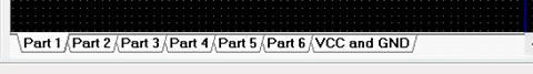
Part 2: Soldering, Desoldering, and Other Tools
Part 3: Solderless Breadboards
D. An Easier Way to Mount Parts
A. Creating Your Own Patterns (Shapes) - The Shape consists of the holes, the pads that will be in the copper, and graphics that will be on the silkscreen. An example of a Shape is a DIP20. And you can turn the Grid off.
B. Creating Your Own Components - In Component Editor you define the graphics that will appear on the Schematic. That includes the component pins with labels and pin numbers. Then you tie it to a Shape. That is so the pin numbers of the component will be tied to the pin numbers on the PC Board.
C. Drawing The Schematic - You can turn the Grid off here too. And don’t forget to use Verification > Electrical Rule Check (ERC)
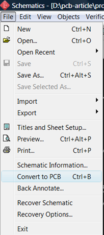
D. Designing the PC Board - With an Actual Example. Includes Making a Ground Plane (Copper Pour) and Removing a Ground Plane (Copper Pour)
Method 1 - Having PCB Designer Do Everything (Auto-Placement and Auto-Routing)
Method 2 - You Do the Placement, PCB designer Does Auto-Routing
Method 3 - You Do the Placement, You Do the Routing
Making a Void in a Solder Mask
Some Other Important Things - Run Verify, Put the Labels on the Layer that You Want Them to Be On
Part 6 - More Useful Software and Some Hardware
A. GerberLogix - Gerber File Viewer
C. RTA - Audio Measurement and Analysis Software
D. External Audio Pods For The Audio Projects
Part 7 - Making the Gerber Files and the Drill File
Part 1 - Introduction
This article is for people who have some experience designing electronic things and building them either with the solderless breadboards that you push wires into (which ends up looking like a game of Twister) or doing wire wrap boards.
The next step is to design printed circuit boards and have them fabricated.
You might think that designing a printed circuit board is too hard and having it fabricated is too expensive.
I hope to show you that you can design a printed circuit board with only some pain and that you can have it fabricated at a very reasonable cost. I will throw in some history while I am at it.
The software that I use is DipTrace (https://diptrace.com/) They offer a free version that is fully functional limited only by the number of pins in the design (300 pins). I am not an expert but I have learned a few things that may make using it easier for you. I will post several projects with schematics and board files that you can modify or just use as is. I will include the Gerber files so if you like my design you can order the boards with them. Note that I use only through-hole devices. I do not do Surface Mount, known as Surface Mount Technology (SMT) or Surface Mount Devices (SMD). And I am doing only two-layer boards. This is not a complete tutorial. It assumes you have some familiarity with DipTrace or can become familiar with it without too much trouble.
I will also list some PC Board fabricators who will make your PC Boards for a reasonable cost.
I hope my article will be useful to those in the Maker Movement. https://en.wikipedia.org/wiki/Maker_culture.
And if you are an Electrical Engineer, knowing how to make things will make you a better Engineer.
Some History - If you are not interested in some history you can skip ahead to Part 2: Soldering, Desoldering, and Tools .
The Maker Movement is not all that new. People have always made things for themselves, even electronic things. For a long time that was the only way to get what you wanted unless you were wealthy enough to pay someone else to do it for you.
If you are a member of the ARRL you can download all of the issues of QST going back to 1916. There is a free site that has some of them: https://archive.org/search.php?query=qst. This one is for January 1955: https://archive.org/details/qstamer00amer. There were lots of things to build.
And there were lots of places to buy parts. Many of the parts were the same parts used in radios (and then TVs) and readily available. You could buy them from Radio Shack. Radio Shack was far from the shell that it is today or was even 40 years ago. Here is a site of old Radio Shack catalogs: http://www.radioshackcatalogs.com/. This one is for 1955: http://www.radioshackcatalogs.com/catalogs/1955/. Tubes, transformers, switches, relays, fuses, resistors, pots, capacitors, variable capacitors. I think it is safe to say that almost anything you could design in 1955 you could get the parts to build it from the Radio Shack catalog.
When you look at the prices in the Radio Shack catalog you should remember that they are 1955 prices. According to the U.S. Department Of Labor Bureau of Labor Statistics at https://www.usinflationcalculator.com/inflation/consumer-price-index-and-annual-percent-changes-from-1913-to-2008/ the Consumer Price Index (All Urban Consumers – (CPI-U) 1913-2018), in June 1955 was 26.7. In July 2018 it was 252.006 for a ratio of 9.44 so, all things being equal, an item priced in 1955 dollars would be 9.44 times as much in today’s dollars. (The baseline of 100 was set for 1984.) Therefore a 6C4 vacuum tube being sold in 1955 for $0.81 would be equivalent to $7.65 today. That’s not bad, but a Harman Kardon AM/FM receiver that went for $189.50 in 1955 would be equivalent to $1,788.89 today (Harman Kardon is now owned by Samsung). But it was a really nice receiver for its time: https://www.radiomuseum.org/r/harman_festival_d_1000.html. A Hammarlund HQ-140 ham receiver cost $264.50 in 1955. This equates to $2,496.89 today. Ouch.
Radio Shack was not the only company that sold parts and equipment. One of the many other companies was Allied Radio. You can see their old catalogs at http://www.alliedcatalogs.com/. This catalog is from 1955: http://www.alliedcatalogs.com/catalogs/1955-140.
There was a magazine for hobbyists and experimenters called Popular Electronics that was published from 1954 - 1985. https://www.americanradiohistory.com/Popular-Electronics-Guide.htm. It was great. Note that today “hobbyists and experimenters” are called Makers. It was in the January 1975 issue of Popular Electronics that the Altair 8800 was introduced. https://www.americanradiohistory.com/Archive-Poptronics/70s/1975/Poptronics-1975-01.pdf. It was billed as the “World’s First Minicomputer Kit to Rival Commercial Models.” That might have been overstating it a little but it was the beginning of the New World. (When the transistor was announced in 1948 it took awhile for it to change the world, too. http://www.rfcafe.com/miscellany/smorgasbord/images/transistor-invention-madison-eagle-july-1-1948-a.jpg)
The magazine Web site has an amazing collection of other magazines as well as many books. https://www.americanradiohistory.com/index.htm. They have most of the issues of Electronics magazine from the first issue in April 1930 through 1958. Hopefully they will be able get the rest of them eventually. (Electronics kept going until 1995.) https://www.americanradiohistory.com/Electronics%20_Master_Page.htm. Although Electronics was a trade magazine it is the history of electronics in the 20th century. (They said much later that they invented the word “electronics” because vacuum tubes used electrons and they felt the word “electrics” wasn’t descriptive enough.) If you want to get a feeling for what it was like not long after the dawn of electronics (with a small ‘e’) read the first issue. https://www.americanradiohistory.com/Archive-Electronics/30s/Electronics-1930-04-Original.pdf.
Most communities had at least one radio/TV repairman who would fix your radio (or TV). Many (probably most) communities had a radio parts store. In the 1960s my goto store was Williams Radio in Edison, NJ. I would go there on my bicycle. Here is a picture of me on my bicycle. Click here. I put a Heathkit Twoer in the front basket. In one of the rear baskets I had a 6V motorcycle battery. This was long before the modern (and tiny) HTs. I also built much of my ham radio equipment for 2 Meters and some for the low bands.
I was a Maker!
In the late 1980s the semiconductor companies started putting out their parts as Surface Mount Devices. Some had through-hole versions. Some did not. That made it difficult to make wire wrap prototypes. You had to go directly to an expensive PC Board. The parts that were programmable (like FPGAs. Microcontrollers, and Digital Signal Processors) needed software tools which the companies decided had to be a profit center, and the software was expensive. That made it difficult to be a Maker unless you worked for a company that could afford the tools. And then you made what your boss told you to make.
Fortunately, things have changed and most of the semiconductor companies have seen the light and provide their software tools for free.
We can be Makers again.
Part 2 - Soldering, Desoldering, and Tools
It might seem odd to start at what is logically the end but if you are like me, as soon as the boards are delivered I want to start stuffing one right away. To do that you have to be prepared. I assume you already have the parts you have designed onto your board.
A. Soldering
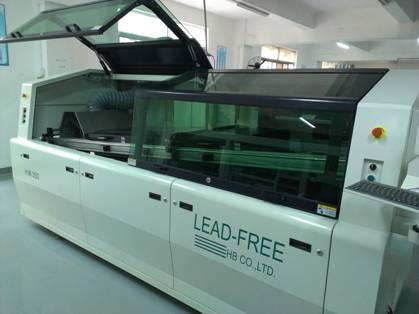
The best way to solder a board is to use a wave solder machine. See https://www.autodesk.com/products/eagle/blog/top-10-soldering-issues-can-ruin-pcb-design/. It contains a description of the process and all the things that can go wrong. This is the basic idea:
The wave soldering process uses a wave soldering machine as shown in the image. This machine is a self-contained oven that takes a bare board with placed components on one end and provides a fully soldered board on the other end. In between this start and end point are several processes, including:
Flux Application. Your board is first placed on a conveyor belt at the onset of the wave soldering machine, and a flux layer is applied. This layer cleans all of your components and ensures that solder can attach properly to the pins and pads on your components.
Preheating. After passing through a flux application, your board then rests on a preheating pad. This process heats your board just enough to prevent any thermal shock before it heads into the soldering wave.
Soldering Wave. This final stage is where your board passes over a liquid soldering wave. The bottom layer of your PCB will make contact with a liquid wave of solder, forming a connection between each component and their associated hole or pad.
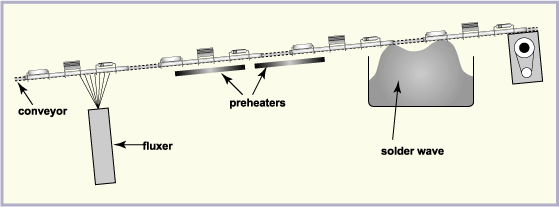
The wave soldering process in visual form, from flux to solid wave. (Image source)
When I was at Atari/Atari Games we used a wave solder machine on our boards. It was awesome.
I don’t have a wave solder machine and you probably don’t have one either. That leaves soldering it by hand with a soldering iron.
The soldering iron that I have used the most often (until recently) for soldering PC Boards has been my trusty Weller SP12 with an MT70 tip.
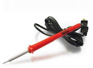
Yes, it is a 12 Watt iron but 12 Watts is all you need as long as the tip is clean and tinned. By “clean” I mean that the tip is not oxidized which is what happens when the metal combines with oxygen from the air. An oxidation layer is a good thermal insulator. And “tinned” means coated with solder because solder contains tin. When the tip is clean and tinned it can reach a temperature of 750 degrees F. That is probably why it oxidizes so quickly.
The traditional way of cleaning the tip is to drag it across a damp sponge. That is what I did for years. When that wasn’t enough I used sandpaper that ground the tip down slightly. When that wasn’t enough (like when I happened to leave it on overnight) I used a file. Eventually the tip would become too short to use and it was time to put in a new tip. Tips are expensive for some reason. It’s a mystery.
Now I use 0000 steel wool, pronounced “4 ought”. That is not to be confused with “40” or “04” . You can get it at Home Depot. It’s really cheap.
https://www.homedepot.com/p/Robtec-Grade-0000-Super-Fine-Steel-Wool-Pads-12-Pack-SWSF12/305600220 .

By using steel wool you also avoid the problem of cooling the tip when your sponge is a little more than damp.
Although the EU has banned the use of solder containing lead I don’t live in an EU country so I still use Sn63/Pb37 solder. That is 63% tin, 37% lead. I use that because that is the eutectic alloy of tin and lead which means it melts at the lowest temperature of the alloy. It is only a little better than the standard Sn60/Pb40 solder. For a chart of the melting temperatures of different solder alloys click here. Note that lead-free solders have a higher melting temperature than leaded solders. That is important because electronic components (especially ICs) can be damaged by excessive heat.
Because of the EU’s ban on leaded solder most ICs and other parts today are tinned with lead free solder. Otherwise companies would have to maintain two separate product flows and two separate inventories. Because they are tinned with lead free solder they require a higher temperature if you are soldering them to a board. Just something to think about.
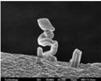
There is another problem with lead free solder: tin whiskers. From November 2006: https://www.appliancedesign.com/articles/91427-metals-and-metal-parts-troubling-tin-tendrils
They're back. The mysterious and
troublesome tin whiskers, once banished, have returned. That's because lead,
the guardian that kept them at bay, has been forced into retirement.
The whiskers that sprout from tin are small, typically no bigger than 1 micron
to 5 microns in diameter, but can grow to several millimeters in length. Though
they are small, they can cause big trouble, enough to turn a $250 million
communication satellite into an orbiting paperweight, and to short circuit
pacemakers, radar systems, relays, GPS receivers, and other electronic
products.
![]()
A single-crystal whisker. Tin whiskers can grow to several millimeters in length and short circuit electronics. Photo: Tyco
In the past, the problem was
successfully mitigated by the use of lead in solder and electroplating. But
with the recent limitations on lead use mandated by the European Restriction of
Hazardous Substances Directive (RoHS) that went into effect on July 1 this year
[2006], using lead as a solution to the problem is no longer an option for most
manufacturers.
Ron Gedney, a retired engineer from IBM, who works on this issue with the
International Electronics Manufacturing Initiative (iNEMI), says that the
problem has been around for 50 years. It was essentially solved decades ago by
adopting a tin-lead composition. "But, take the lead out of everything,
and back comes tin whiskers," he says.
Tin whiskers are single crystals of tin that spontaneously grow from the
surface of tin and tin alloy platings, says Robert D. Hilty, technology
director, Materials Research, Tyco Electronics. The whiskers can take many
shapes, can bend and kink during growth, and grow to lengths as long as several
millimeters. They can grow through finishes. They grow in room ambient
conditions and seem to grow faster in hot and humid environments. They have
also been grown in vacuum chambers meant to replicate space conditions.
Whisker length becomes a problem when they grow long enough to come in contact
with other electrical leads, creating electrical shorts. This is believed to
have been the cause of a wide range of product failures, including the
disabling of the Galaxy 4 communications satellite in 1998. In studying tin
whiskers, NASA duplicated what may have happened in that case by creating tin
whiskers in a vacuum chamber.
Most manufacturers, with the exception of some aerospace and military suppliers
who are exempt, are already working in a lead-free environment and are now
using the best mitigation practices available. Nonetheless, the problem is not
going away. It is believed that whiskers will eventually grow in most products
- over a period of a day, a week or even years - and researchers are looking
for ways to retard their growth or design products that will not be affected by
their growth.
See also: https://en.wikipedia.org/wiki/Whisker_(metallurgy)
The problem that Toyota had several years ago with unintended acceleration of their vehicles was probably due, at least in part, to tin whiskers on their electronic throttle controls. The problem was bad enough that NASA got involved, presumably because of their considerable experience with sensors. For their report click here. Toyota may have also had poorly written firmware. For that report click here.
In order to make a good solder joint the two (or more) metal pieces have to be very clean. If you are soldering two copper wires and one (or both) are oxidized you will not get a good solder joint. In fact you might not get a soldered joint at all. Soldering was, and still is, used to join copper pipes. A flux (a chemical cleaning agent) commonly containing acid (and applied with a brush) is used to clean the surfaces for soldering. Afterwards, it has to be carefully removed since acid is corrosive. This would have been very inconvenient when electronics came along with all of its wires and terminals. So they came up with rosin flux. From: https://hackaday.com/2017/02/23/what-the-flux-how-does-solder-work-anyway/:
Electronic solder usually has a flux made of rosin. Rosin is a natural product derived from pine trees, notably the loblolly and longleaf pines for US-made rosin. It has the advantage of being more or less inert at room temperature but highly acidic when liquified, and has a melting point slightly lower than solder. The rosin core of electronic solder will therefore melt before the solder, flowing into and around the joint. The acidic liquid reacts with metal oxides, exposing clean metal for the solder to wet into. The acidic liquid flux converts the metal oxides to metal salts and water, which are typically locked up in the flux when it solidifies. The reaction products are generally harmless at that point, but some processes still require the used-up flux to be removed.
Solder for soldering electronics has the flux inside the solder at its core. Hence the name rosin core solder.
Here’s a tip. If you are adding a wire to an already-soldered connection you should tin the new wire with new solder and add some new solder to the old soldered joint because the old soldered joint doesn’t have any rosin in it.
After you are done soldering your board you should clean off the flux left behind. I use acetone. It works really well. It dries fast and does not leave a residue. Acetone is a very good organic solvent. It will dissolve many types of plastic. Jars that are safe are: metal, glass (like a glass baby food jar), Polypropylene (PP) and high-density polyethylene (HDPE). And keep it sealed when not in use. Acetone evaporates easily. And try not to get it on yourself. I don’t know how long it will take to dissolve your skin, it will irritate it first. That should motivate you to wash it off.
Apparently I am being politically incorrect. You are supposed to use isopropyl alcohol. I have found it slower to dry, probably because standard isopropyl rubbing alcohol contains water. When you buy 70% isopropyl alcohol the other 30% is water. You can buy 90% isopropyl alcohol in regular stores so it contains only 10% water. I have also found that isopropyl alcohol leaves a film behind. You will have to decide for yourself which to use. If you decide to use acetone you can get it at Home Depot, Walmart, and just about anywhere they sell paint. And despite some comments I have found on the ‘Net acetone does not dissolve my solder masks.
Whichever you use, you need a brush. I use a brush like this:
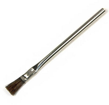
Its technical name is “horsehair bristle acid shop brush.” You can get them really cheap at Harbor Freight Tools: https://www.harborfreight.com/36-pc-12-in-horsehair-bristle-acid-shop-brushes-61880.html . I take one and cut the bristle leaving about 1/4" of bristle left on the brush. That makes it very stiff so it can brush off the rosin.
Some History
In the old days PC Boards were cleaned using Freon which is a chlorofluorocarbon (CFC). Freon is a great cleaner. And it was very cheap. It was also used in Freeze Spray to cool down electric components to see if one of them was temperature sensitive enough to cause the problem you were trying to find. The Freon was stored in the can at high pressure so it was still a liquid. When it was allowed to expand to normal atmospheric pressure to become a gas it became very cold. That is why it was used in refrigerators and air conditioners.
Because Freon was so cheap, after being used to clean PC Boards the Freon (now contaminated with the rosin it had removed) was vented to the atmosphere. I believe that’s what we did at Atari.
But even before CFCs were banned (it became illegal to make it or bring it into the U.S., but not to use it if you already had it) the cost started going up. The manufacturers developed a system to capture the used Freon, clean it up, and use it again.
Atari didn’t do that because there was another system that cleaned the boards with just deionized water. That’s what we went to.
I found this reference: An Assessment of Alternatives for Replacing Freon 113 in Bench-Type Electrical Circuit Board Cleaning at Fermi National Accelerator Laboratory issued December 1993. Click here. On PDF page 22 it cites an article in Electronics:
A January 1991 issue of Electronics indicates that no less than 20% of ODS emissions is caused by cleaning processes of electronic circuit boards and other electronic gear. (p. 1)
(ODS means Ozone Depleting Substances.)
It also says that the military resisted giving up CFC-113.
Eventually they did. Now, according to MIL–PRF–31032B w/AMENDMENT 1 16 May 2012 PERFORMANCE SPECIFICATION PRINTED CIRCUIT BOARD/PRINTED WIRING BOARD, GENERAL SPECIFICATION FOR (Click here):
F.5.2 Flux. When flux is used, it shall conform to type R0L1 of J–STD–004, or as specified in the applicable performance specification or MIL–PRF–31032 specification sheet.
F.5.3 Solvent. A solvent, such as isopropyl alcohol, suitable for flux removal following the solder float tests.
The solder float test simulates high temperature wave solder.
Also note that they require the use of leaded solder:
F.5.1 Solder. The solder or solder paste shall be tin-lead alloy with a nominal tin content of 50 percent to 70 percent in accordance with J–STD–005 or J–STD–006. When specified in the applicable performance specification or MIL–PRF–31032 specification sheet, other solders can be used provided they are molten at the specified temperature.
I think that is very wise. You don’t want to facilitate the growth of tin whiskers in your military equipment. I wonder if the EU countries have an exception for the U.S. military equipment that they buy.
Safety
And now let’s talk about safety.
1. First, wear protective glasses when you are soldering. There are conditions where solder can splash onto your face. That happened to me once when I was unsoldering parts on a board (and I was tired and careless).
2. When you are soldering you will have fumes from the solder and from the flux being melted. And since you are soldering little things you will probably be soldering them up close so the fumes will go into your face.
The safest way to solder is in a fume hood.
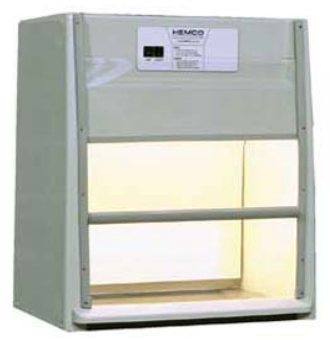
This is a Hemco 92011 and costs only $1,426. Oh.
You could probably build something like it that would work satisfactorily. A box with everything sealed except for the front, some glass so you can look into it and not get fumes in your face, a good blower, and a filter. Then you should vent it outside. Or maybe you could use a HEPA filter that is good enough that you can vent it back into the room a few feet away. Maybe you can tilt the glass so you can look straight through it. (Seal the sides.) Maybe the platform inside the box can have an adjustable tilt so you can see the board straight on. And maybe a magnifying glass so us old folks can see the board. And the inside should be well lighted. Run the blower and the lights on low voltage DC (like 12VDC or 24VDC) so you won’t have Mains voltage in your box.
I don’t have a fume hood. I have never had a fume hood. Nowadays I have a small blower on my bench that sucks the fumes away.
If you are pregnant, plan to become pregnant, or are nursing you should protect yourself better than I do.
And BTW, I am seeing pictures of the SP12 that look different from mine.
Hopefully it is not a counterfeit and it was Weller who redesigned it. The new triangular shape at the collar would let you put it down on a surface and it won’t roll around. Except that when you are not soldering with it you should put it in a holder. Nonetheless the triangular shape is a good idea. Why did they wait so long to do it? (I got my first SP12 about 25 years ago.)
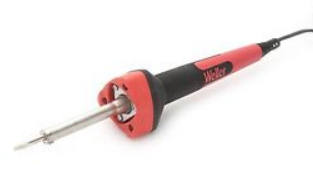
I became more aware of soldering temperatures last year when I bought my first temperature-controlled soldering iron, a TENMA 21-10115 Soldering Station, 110 VAC, 896 °F, 60 W, LCD Display, Solder Iron, Sponge, US.
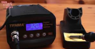
It was on sale and I couldn’t resist it. For the manual click here.
Once I got it I had to decide what temperature to set it to. I started low (about 361 degrees F) because that is the melting temperature of my solder. That didn’t work when soldering parts to a PC Board. I kept increasing it until I was happy with my solder joints and have ended up at 572 degrees F which is one of the three preset temperatures. You can also set it to any temperature you want between 302°F and 842°F. The tip comes with the note (click here):
The 21-10148 is a 0.5mm Conical Soldering Tip made of copper and alloy iron coated iron tips perform excellent on temperature between 360 and 380°C. It can only work 4 to 5 hours if tips continuously get heated up beyond 450°C and chrome layer will lose effect if temperature is up to 500°C. It is suitable for use with 21-10115, 21-10120 and 21-10130 soldering stations.
Note that the temperatures are in Celsius. I have been using my iron at 572 degrees F (300 degrees C) for almost a year and my tip is still very good. The SP12 at 750 degrees F is 399 degrees C which explains why it oxidizes faster.
There are other companies who make temperature controlled soldering irons, but be careful. Some soldering irons look like they might be temperature controlled but are not. They only use a triac to control the power. I consider that completely useless. If it doesn’t say temperature-controlled then it isn’t. And whatever you buy make sure you can buy tips for it.
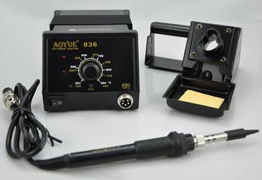
There are several companies that make clones of the now-discontinued Hakko 936 (https://www.hakkousa.com/products/soldering/936-esd-soldering-station.html). These companies are Aoyue, Gaoyue, Yihua, and others without names.
They have a knob (on a pot) for setting the temperature. They have another control for calibrating the temperature knob. How do you measure temperatures like 571 degrees F? You need something with a thermocouple. I bought one on eBay several years ago called Digital Thermometer Type K 6802. They are still sold on eBay at prices as low as $22. But unless you have another use for the thermocouple thermometer, if you add it to the cost of the clone soldering iron you could be up to the cost of a temperature controlled soldering iron with a temperature display.
I have an idea. If the soldering iron really is temperature controlled then it knows the temperature. All it needs is a way of communicating it. It has an LED. It can flash the temperature numbers like 5 flashes - pause - 7 flashes - pause - 1 flash. I have a universal remote control that has a mode that does that so you can read the codes for the devices you have programmed it for. It would need a pushbutton switch so you can turn that function on and off. Otherwise it would be really annoying. That would require one input to the microcontroller. Ok, maybe two bits if they are running the LED from the same bit they are using to turn the heating element on and off. It might already have that. A display would need more bits.
If you don’t do a lot of soldering I recommend the Weller SP12. If you do a lot of soldering I recommend the Tenma 21-10115 or something equivalent to it. Whatever soldering iron you buy get one or two extra tips for it when you buy it.
But if you want a really serious soldering iron I recommend this American Beauty: https://americanbeautytools.com/Soldering-Irons/19
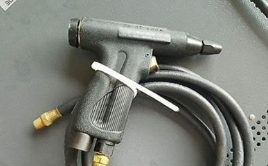
B. Desoldering
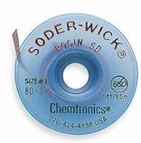
Sometimes you have to desolder a joint. For years I used solder braid or a manual desoldering pump.
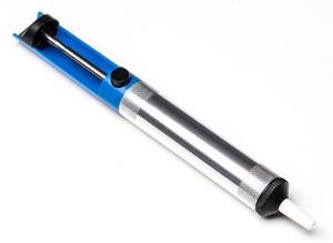
I also have one of these but it has never worked for me very well.
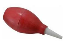
For some reason the solder braid and hand pump don’t work very well on the PC Boards that I have been stuffing for the past year or so since I have been having PC Boards fabricated again.
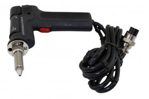
So I broke down and bought a CSI474A Desoldering Station from Circuit Specialists: https://www.circuitspecialists.com/Compact_Desoldering_System.html .
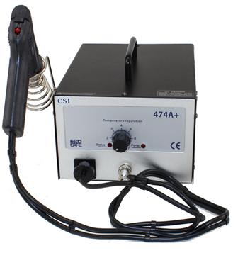
This appears to be a version made for Circuit Specialists of the 474A Desoldering Station which is made by and for other companies as well.
I love it. Now I can desolder parts from my PC Boards without having decide whether to sacrifice the part or the board.
It is important to clean the solder out of the 474A or it will get clogged up. If it gets clogged up it won’t work. It is best to clean it every time before you use it. Or you can clean it every time after you use it but it will be hot.
There is a small filter at the end of the barrel that keeps the solder from going into the pump.
There is a metal spring in the barrel to catch the solder. It gets clogged up.
And sometimes I get the tip of the gun clogged.
For that they give you a small drill bit (0.035” which is the typical size of a small PC Board hole). It has a long shaft so use it by hand. It comes with a holder. If you put it in a drill you will break the drill bit. The drill bit is also useful if there is still a small amount of solder left in the hole and you need a completely clear hole.
And try not to lose the rubber grommet at the front of the barrel.
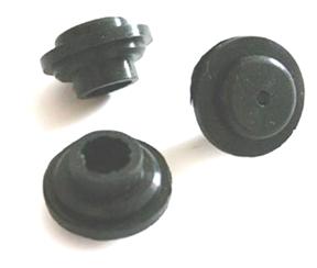
I lost one when it got away from me, took a bounce or two, and I couldn’t find it. The CSI 474A comes with a spare but that meant I no longer had a spare. CSI does not sell the part but they found one lying around and sent it to me for the cost of shipping. This part is also used in Aoyue’s version of the desoldering station. They call the part the “AOYUE 3024X Filter Pipe Cover Aoyue 474/701/2702/”. I found it on eBay at a reasonable price from a company in Spain.
Since I bought my CSI 474A they have raised the price. By the time you read this the Aoyue 474 might be a better deal. Shop around.
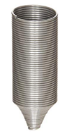
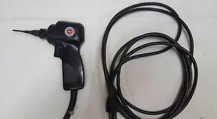
And I have found a desoldering iron that costs less and works better for me. I found it on eBay where it is called: 110V 115V 120V 40W Electric Desoldering Iron Pump Vacuum Solder Sucker 40 watt and it looks like this:
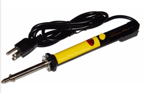
It is a soldering iron with a hole through the center and has a manually operated solder sucker. You push the plunger down to cock the spring, hold the tip against the joint to unsolder, wait for it to melt the joint, and press the button. It does a good job sucking up the solder. To use it, clean the tip with 0000 steel wool. This is very fine steel wool. Then tin the tip with solder. This sounds like the wrong thing to do but tinning the tip helps transmit the heat to the joint to be unsoldered. It doesn’t use those expensive little sponge filters. It doesn’t use any filters. The solder that it sucks up is ejected when you push the plunger down. So don’t push the plunger down over your board. :-(
A Short History of Soldering (and Alloys)
Soldering is not welding. From https://en.wikipedia.org/wiki/Welding
Welding is a fabrication or sculptural process that joins materials, usually metals or thermoplastics, by causing fusion, which is distinct from lower temperature metal-joining techniques such as brazing and soldering, which do not melt the base metal.
Soldering is similar to brazing but brazing uses a higher temperature which produces a stronger joint. From: https://en.wikipedia.org/wiki/Brazing
Brazing is a metal-joining process in which two or more metal items are joined together by melting and flowing a filler metal into the joint, the filler metal having a lower melting point than the adjoining metal.
Brazing differs from welding in that it does not involve melting the work pieces and from soldering in using higher temperatures for a similar process, while also requiring much more closely fitted parts than when soldering. The filler metal flows into the gap between close-fitting parts by capillary action. The filler metal is brought slightly above its melting (liquidus) temperature while protected by a suitable atmosphere, usually a flux. It then flows over the base metal (known as wetting) and is then cooled to join the work pieces together.[1] A major advantage of brazing is the ability to join the same or different metals with considerable strength.
From: https://en.wikipedia.org/wiki/Soldering
Soldering (AmE: /ˈsɒdərɪŋ/, BrE: /ˈsoʊldərɪŋ/), is a process in which two or more items (usually metal) are joined together by melting and putting a filler metal (solder) into the joint, the filler metal having a lower melting point than the adjoining metal. Soldering differs from welding in that soldering does not involve melting the work pieces. In brazing, the filler metal melts at a higher temperature, but the work piece metal does not melt.
Solder
Here is everything you would want to know about solder. https://en.wikipedia.org/wiki/Solder
Solder is an alloy. Until recently it was usually an alloy of tin (Tn) and lead (Pb). Alloys are interesting. An alloy is a combination of metals or of a metal and another element. They do not produce a new molecule. The constituents are still there in their original form but the alloy can have very different (and useful) properties than the constituents. Indeed, the proportion of the constituents can give the result different properties.
Some examples:
1. Bronze is an alloy consisting primarily of copper, commonly with about 12% tin and often with the addition of other metals (such as aluminum, manganese, nickel or zinc) and sometimes non-metals or metalloids such as arsenic, phosphorus or silicon. These additions produce a range of alloys that may be harder than copper alone, or have other useful properties, such as stiffness, ductility, or machinability. https://en.wikipedia.org/wiki/Bronze
Bronze was so important that an entire Age of Humankind is named for it: the Bronze Age. From https://en.wikipedia.org/wiki/Bronze
The beginning of the Bronze Age in India and western Eurasia is conventionally dated to the mid-4th millennium BC, and to the early 2nd millennium BC in China;[1] everywhere it gradually spread across regions.
2. Brass is an alloy of copper and zinc. From https://en.wikipedia.org/wiki/Brass
Brass has higher malleability than bronze or zinc. The relatively low melting point of brass (900 to 940 °C, 1,650 to 1,720 °F, depending on composition) and its flow characteristics make it a relatively easy material to cast. By varying the proportions of copper and zinc, the properties of the brass can be changed, allowing hard and soft brasses.
Brass did not start being used until Roman times at the earliest. Does that mean that while early humans knew about tin (and had access to it) they either didn’t know about zinc or didn’t have any? From https://en.wikipedia.org/wiki/Zinc
To date, the oldest evidence of pure zinc comes from Zawar, in Rajasthan, as early as the 9th century AD when a distillation process was employed to make pure zinc.[8] Alchemists burned zinc in air to form what they called "philosopher's wool" or "white snow".
I guess they didn’t have much of it until they found it in Zawar, a settlement located in Udaipur district, Rajasthan, India.
3. Wrought Iron. From https://en.wikipedia.org/wiki/Wrought_iron
Wrought iron is an iron alloy with a very low carbon (less than 0.08%) content in contrast to cast iron (2.1% to 4%). It is a semi-fused mass of iron with fibrous slag inclusions (up to 2% by weight), which gives it a "grain" resembling wood that is visible when it is etched or bent to the point of failure. Wrought iron is tough, malleable, ductile, corrosion-resistant and easily welded. Before the development of effective methods of steelmaking and the availability of large quantities of steel, wrought iron was the most common form of malleable iron. It was given the name wrought because it was hammered, rolled or otherwise worked while hot enough to expel molten slag. The modern functional equivalent of wrought iron is mild or low carbon steel. Neither wrought iron nor mild steel contain enough carbon to be hardenable by heating and quenching.[1]
4. Mild or low-carbon steel. From https://en.wikipedia.org/wiki/Carbon_steel#Mild_or_low-carbon_steel
Mild steel (iron containing a small percentage of carbon, strong and tough but not readily tempered), also known as plain-carbon steel and low-carbon steel, is now the most common form of steel because its price is relatively low while it provides material properties that are acceptable for many applications. Mild steel contains approximately 0.05–0.25% carbon[1] making it malleable and ductile. Mild steel has a relatively low tensile strength, but it is cheap and easy to form; surface hardness can be increased through carburizing.[3]
Note that mild steel can have less carbon than cast iron and more carbon than wrought iron. Why didn’t they just make mild steel?
The answer is that steel is not just the proportion of the constituents. It is the process used to make it. https://en.wikipedia.org/wiki/Steelmaking
The process for making steel requires more heat than it is practical to get from wood. The solution did not come about until late in the 16th century. It’s called coke (no, not that kind). Coke is produced by heating coal in the absence of oxygen. https://en.wikipedia.org/wiki/Coke_(fuel). Then you burn the coke, which is a denser fuel with fewer impurities (and produces less smoke) than the original coal.
The use of coke has been declining for some time, being replaced by natural gas.
https://www.thespec.com/news-story/4190319-u-s-steel-natural-gas-process-will-soon-replace-coke/
The melting temperature of tin is 231.9 degrees Celsius. The melting temperature of lead is 327.5 degrees Celsius. The melting temperature of Sn60Pb40 solder is 183-190 degrees Celsius. The melting temperature of copper is 1,085 degrees Celsius. My soldering iron does a good job soldering to copper at 300 degrees Celsius. How is it that you can solder tin/lead to copper when the copper isn’t melted during the process? I found the answer at https://www.howcast.com/videos/504745-how-does-solder-get-inside-copper-soldering/
Soldering and brazing are two techniques of joining metals where the base metal, in the case of electronics which is copper, the base metal doesn’t actually melt and it’s natural to ask how does the solder get inside of the copper if the copper doesn’t melt?
Now, copper is a metal that’s not made of a pure single crystal but is formed of lots and lots of small micro crystals. We call it a polycrystalline material. And in between these crystals are little spaces where the tin and lead from solder can diffuse into cracks and crevices, microscopic crevices and useful to form the bond. So the tin lead doesn’t really get into the crystal structure itself of copper but gets in between the crystals. And the same is true for brazing as well.
So if you were to look at the material under a microscope you’d see lots and lots of little grains of salt, if you will. And if you were to look at a microscopic image of soldered copper you’d see that the solder flows in between the crystals and leaving little islands of copper in between.
Much of the soldering takes place at the microscopic scale. Things like these oxides that disrupt solder are little particles that get in between the solder and the copper and prevent this diffusion of lead and tin into the crevices of copper. So there’s a lot going on at the microscopic scale. It’s very important to the features that we’re interested in at much larger scales.
And you can look at a piece of soldered material. If you were to cut it you’d see a layer of tin lead and a very sharp line where the copper begins. But look closely at that layer and you’ll see the that the tin and lead are actually intermingling with the copper and so there’s a boundary layer where the tin and lead have flowed into the copper a short distance but you’ll see that there’s actually a zone where the two metals exist but the three metals exist all together.
Why can’t I solder iron? It turns out you can (at least cast iron) but it isn’t easy and it needs the higher temperature of a propane torch: https://www.hunker.com/13415175/how-to-solder-cast-iron
Here is a chart of the solderability of different metals. http://www.efunda.com/materials/solders/solderability.cfm
I am glad that all I have to solder is copper.
C. Other Tools
In order to stuff the components on the board you may have to form the leads such as with resistors. You can do it by hand with long-nose pliers but that takes some time to get the spacing right and there is an easier way.
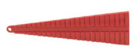
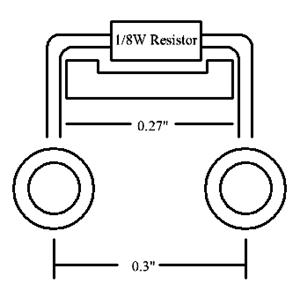
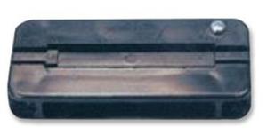
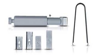
I have two tools that look like this:
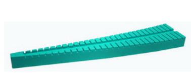
One is for a 1/4W and 1/2W resistors, the other is for 1/8W resistors. The channel is wide enough for the resistor. You select what lead spacing you want. For 1/4W resistors it is usually 0.4”. For 1/8W resistors it is usually 0.3”. Then you bend the leads down. That should be easy.
I bought my benders several decades ago. The company whose name is on them no longer exists (The Granite Corporation. Los Angeles, CA.) or if they do, they no longer make tools for the electronic industry.
I have found benders from several sources.
Techno-tools sells these:
Techni-Tool Part # 802 for 1/8W resistors: http://www.techni-tool.com/664SO802

Techni-Tool Part # 801 for 1/4W and 1/2W resistors: http://www.techni-tool.com/664SO801
Jameco sells one that looks just like the Techni-Tool one for 1/4W resistors.
https://www.jameco.com/z/801-Lead-Forming-Tool-for-Resistors-and-Capacitors_106884.html
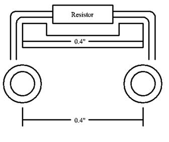
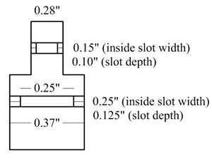
I was buying some other parts from Jameco so I bought theirs so I could report on it. I am sorry to report that it is a piece of crap. It is designed wrong.
When I bend the leads on my resistors I want the bent leads to fit in the center of the holes on my board. Jameco’s bender does not take into account the diameter of the leads. The slot for 0.4” spacing is indeed 0.4”. As a result the bent leads are too wide by the diameter of one resistor lead. I have exaggerated the following two figures somewhat for clarity.
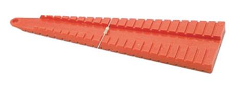
Jameco’s bender.
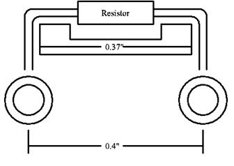
My bender has a width of 0.37”.
The bender from Techi-Tool looks like Jameco’s. I don’t know if it is also wrong.
I only need two slots, one for a 1/4W resistor with a 0.4” footprint (shown above) and one for an 1/8W resistor with a 0.3” footprint.
Maybe someone with a 3D printer could make some. Give them to your friends. Or use your 3D printer to make a mold and have them molded. Sell them for $1.50 and you will be a millionaire before you know it.
1. This is not to scale and the dimensions might not be exactly precisely right.
2. It would be nice if the corners that bend the leads are rounded.
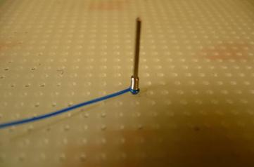
Another tool you need is for bending the integrated circuit leads.
The leads on an integrated circuit are somewhat springy metal splayed outwards a little. That is so they can be bent inwards to fit the footprint, then released so they spring back so they are held on the board.
Here is an example
You can bend the leads using the brute force method by bending the pins against a flat surface.
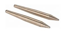
Or you can use this tool called: IC Pin Straightener, Static Grounded.
One side is for 0.3” ICs, the other side is for 0.6” ICs (like old EPROMs) which are not used very much anymore.
It also straightens the pins if they have gotten out of line.
Two sources are Newark:
and Jameco:
Note that even with this tool you need some care in inserting the IC.
There is also the old Radio Shack insertion tool which the IC fits into. Then you put the IC in the socket (or in the board) and press the button which forces the tool off of the now-inserted IC. It also comes with the IC extractor on the right side of the picture which I have never been able to use without bending the shit out of the IC pins.
As I write this you can still get them on Amazon for less than $10.
If you are putting an IC in a socket and you manage to bend and scrunch a pin you can usually straighten it with long-nose pliers without breaking off the pin. The second time you bend that pin and try to straighten it the pin will almost certainly break off. That sucks if it is an expensive IC, or your last one of that type.
About sockets.
1. With prototypes I usually put ICs (other than voltage regulators) in sockets.
2. I always use sockets with machine tooled pins, not the cheaper ones with leaf springs. I don’t trust them.
Sockets with machine tooled pins aren’t cheap but you can get them at a reasonable price from https://www.taydaelectronics.com/catalogsearch/result/?q=ic+socket .
They are one of my goto suppliers.
Wire wrap sockets are even more expensive. I get mine from Phoenix Enterprises: https://www.peconnectors.com/wire-wrap-sockets-and-headers/.
Here is a tip when doing wire wrap.
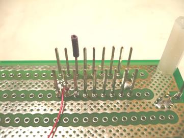
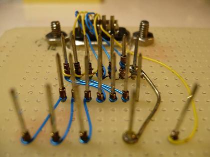
If you are using a 14-pin logic DIP use an 18 pin socket. You put a 0.1uF bypass capacitor in pins 18 and 17. Ground Pin 18. Pin 17 will connect to pin 16 which will be the IC pin 14 (VCC). I then slip a small piece of insulation over pin 3 to indicate that it is now IC pin 1.
This is the top, using one of the prototype boards I am presenting later. There is room for another component in the socket.
This is the bottom. The red wire is for +5V.
If you are using a 16-pin logic IC use a 20-pin socket. You put a 0.1uF bypass capacitor in pins 20 and 19. Ground Pin 20. Pin 19 will connect to pin 18 which will be the IC pin 16 (VCC). I then slip a small piece of insulation over pin 3 to indicate that it is now IC pin 1.
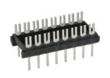
You can get 24-pin wire wrap sockets (0.3” wide) so your 20-pin logic DIPs won’t feel left out.
Part 3: Solderless Breadboards
I have used them a few times. I don’t care for them. They end up looking like a game of twister. And if you don’t use the proper size wire it either doesn’t make reliable contact or it bends the spring contacts.
Part 4: Wire Wrap
The basic idea of wire wrap is that you have a square post with good corners. When you wrap the wire around it with the proper tension the corners bite into the wire and make a gas-tight connection to the post. No soldering is required.
Wire wrap was invented by Western Electric for the Bell System (“The Phone Company”). (https://en.wikipedia.org/wiki/Wire_wrap) Here is probably everything you need to know about it. Click here. It is from Gardner-Denver who worked with Western Electric in developing wire wrap.
Western Electric generally used 22 AWG or 24 AWG wire on posts that are 0.045” square.
It was adapted by IBM to make its computers. They used 30 AWG wire on 0.025” posts. It is IBM’s system that is used today in electronics.
For some reason many of the wire wrap tools available on eBay are for the Western Electric standard (24 AWG wire on 0.045” posts). More about that in a little bit.
A. Wire Wrap Tools
There are several types of wrapping tools.
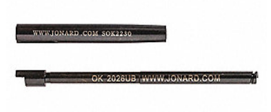
This one you use by hand. One end is for wrapping, the other end is for unwrapping. This is a WSU-30M made by Jonard Tools/OK Industries.
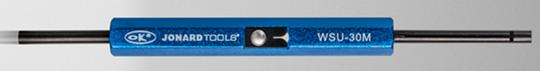
I don’t recommend wire wrapping by hand. If you wrap more than a few wires you will wreck your hand. However, you will occasionally need to unwrap a wire either because you are changing the design or you put the wire on the wrong post. You will need an unwrapping tool, either this one or one that just does unwrapping.
This wrapping tool is also hand operated.
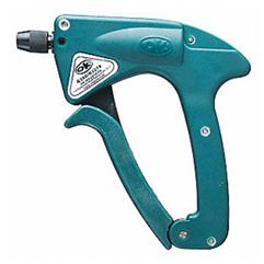
You squeeze it. I don’t recommend it either. It will wreck your hand too.
There are battery operated wrapping tools.
Meh. I want something that doesn’t need batteries.
There are powered tools that run on compressed air.
That might be ok in an industrial environment and the pneumatic motor will probably last forever. That’s more than I need.
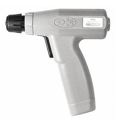
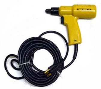
I use one that runs on the Mains. It looks like this.
Mine was already old when I bought it at an auction for $5 about 25 years ago. After several years it started to run slowly. I took it apart and lubricated everything that looked like it would benefit from being lubricated. That brought it back.
Two years ago it started running slow again. This time lubricating it didn’t help.
I turned to eBay and learned a lot about wire wrap tools.
The powered tools need to use the proper bit and sleeve.

They can use a large variety of bits and sleeves. Click here for this reference from Cooper Industries. See the table on PDF page 5. http://www.cooperindustries.com/content/public/en.html says they are now owned by Eaton. I don’t see any wire wrap tools on their Web site.
I use a 519936 Bit with a 507100 Sleeve. These may be old numbers that are not easily available.
Here is another source for bits and sleeves.
http://www.jdvproducts.com/wire-wrapping/bits-sleeves/3-modified-wrap-bits/flypage.tpl.html
This bit looks promising: A Jonard SB30MSH-B for 30 AWG and a maximum post diagonal of 0.031”. That would be a post that is 0.025” on a side.
The compatible sleeve is their Part # P3032.
This is the same part number used by OK Industries, probably because Jonard bought the OK Industries’ wire wrap product line in 2003.
I have not bought and tested the above Jonard/OK Industries parts so I cannot guarantee that they will work.
If you are lucky you may be able to find them on eBay at a reasonable price.
Two years ago I bought a JDV Standard Pneumatic 6021 Electric Wire Wrap Gun on eBay for a good price. The seller said he didn’t know if it was new or not. It looks new to me. It looks like this.
Some wire wrap guns on eBay come with a bit and sleeve. They might or might not be the correct bit and sleeve for 30 AWG and 0.025” posts. The sellers usually don’t say. They might not know about bits and sleeves.
B. Wire Wrap Wire
Use 30 AWG Kynar wire. Kynar is the type of insulation and is a trademark of Arkema, Inc. (https://www.arkema.com/en/) It was originally developed by Pennsalt Chemicals Corporation. Click here.
Kynar is a Fluorine-Containing Synthetic Resin which makes for very tough insulation. Click here.
The wire that is used is silver-plated copper. The silver plating is not very thick but it makes very good contact with the posts. However, since it is silver it will tarnish fairly quickly when exposed to air. Quickly means a few weeks to a few months depending on humidity and air pollution (like containing sulfur).
It doesn’t matter because the wire wrap connections to the posts are gas-tight.
You can buy Kynar wire wrap wire in precut prestripped lengths. Why would you spend the money for that when you can buy the wire (which comes in several different colors) and cut and strip it yourself? That way you get whatever length you need as many times as you need it.
To properly strip the wire use the Claus No-Nik 0.14” (or NN014) wire stripper. It has dark green handles.
They make ones for stripping other size wires. They have different color handles.
On eBay many of the sellers call it a Fiber Optic Stripper. I don’t know where they got that from. The NN014 is for stripping 30 AWG Kynar wire.
BTW, when you strip a wire it sometimes leaves behind a small piece of insulation in the V-groove. You need to remove it or the next wire won’t be stripped properly. You can remove it (most of the time) by opening the handle and rapping it gently on a hard surface (like your work table).
To wrap a wire you strip it about 1”. The small hole in the wire wrap bit is for the wire. The large hole is for the post. Put the wire in the small hole. Put the large hole around the post (or put the post in the large hole depending on your frame of reference). Pull the trigger.
C. More Tools
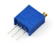
You will need a small flat bladed screwdriver with a 2mm tip in order to adjust the trimpots which you will probably use.
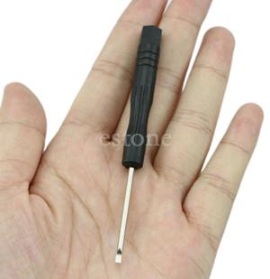
On eBay do a search for Screwdriver 2mm Slot Type.
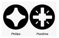
Pozidriv
And since we are on the subject of tools there is something you should know.
Many items from China, even consumer items, use screws that look like Phillips head screws but they aren’t. Phillips head screwdrivers do a poor job or don’t work at all. It is very frustrating. A few years ago I bought a White Rodgers thermostat where the screws on the connection block were impossible to turn with any of my Phillips head screwdrivers. I thought the screws were improperly made.
It turned out that they were not Phillips head screws. They were Pozidriv screws that required their own Pozidriv bits.
Phillips head screws were invented by John P. Thompson who sold the rights to Henry Frank Phillips who was a U.S. businessman from Portland, Oregon. https://en.wikipedia.org/wiki/Henry_F._Phillips. (It was not invented by or named after Philips, the giant Dutch conglomerate.)
What Wikipedia doesn’t say is that the Phillips head was designed so that too much force would cause the driving bit to come out of the head. This was to keep excessive force from damaging the work or causing the screw to shear off. Since this was before screwdrivers (like electric screwdrivers) were available with torque limiting it was a good idea.
From: https://www.finehomebuilding.com/2015/09/16/what-is-the-difference-screw-bits-phillips-vs-pozidriv (written by Matt Higgins):
Phillips
The key improvements of the Phillips system over the slotted system are that its bits self-center and will cam out (slip out) when a fastener is sufficiently seated. On a production line, these features are huge time savers. The most common Phillips sizes are 1, 2, and 3 (from smallest to largest), and the bits typically have “ph” indicated on them. The patent on the Phillips design expired in 1966, but the Phillips Screw Company has continued to improve on the cruciform-shaped drive, which has led to other drive systems from the same company, such as the Pozidriv.
Pozidriv
When trying to tighten up that previously mentioned cup hinge with a Phillips bit, you probably should be using a Pozidriv. The Pozidriv also has a self-centering design, but the shape is modified for improved engagement. The sure sign that a screw is Pozidriv is the four tick marks or indentations around the cross. Viewed from the side, the difference between Phillips and Pozidriv bits is unmistakable. A Pozidriv has ribs between each of the four arms of the cross. This adds the increased grip. A Phillips bit fits in a Pozidriv screw head, but it will most likely cam out before the fastener is fully tight. This can damage the fastener and is why that cup hinge loosens up so quickly when a Phillips bit is used. A Pozidriv bit does not fit in a Phillips screw. Pozidriv bits are available in driver sizes from 0 to 5 (from smallest to largest) and have “pz” marked on them.
One way to get Pozidriv bits is from Zoro: https://www.zoro.com/search?q=pozidriv&sort=variants.price:LowtoHigh
I got mine from Zoro but through Walmart even cheaper:
https://www.walmart.com/ip/159501147 Irwin Screwdriver Bit, Stainless Steel, 3052022 (Irwin #1 Pozidriv)
https://www.walmart.com/ip/41904839 Irwin Screwdriver Bit, Stainless Steel, 3052023 (Irwin #2 Pozidriv)
https://www.walmart.com/ip/273671295 Irwin Screwdriver Bit, Stainless Steel, 3052024 (Irwin #3 Pozidriv)
You use them with a standard 1/4” driver.
Buy a bunch and give them to your close friends.
I recently bought a pack of screwdriver bits off the rack at my local Walmart (in Reno) that contained some Pozidriv bits. “Hyper Tough TS99876A 32-Piece Screwdriver Bit Set” for $5.88. It includes Pozidriv bits PZ0, PZ1, PZ2, and PZ3. It also contains several Tamper Proof Star Bits (Torx Security Bits). https://www.walmart.com/ip/HYPER-TOUGH-TS99876A-32-PIECE-SCREWDRIVER-BIT-SET/870311412
D. An Easier Way to Mount Parts
The standard way to mount parts for a wire wrap board is to use a DIP Adapter Header. You solder the parts onto the header and then you plug the header into a wire wrap socket. It looks like this:
They make for a very secure way to mount parts. The parts are not going to fall out. The problem I have with them is:
1. They cost way too much; and
2. If you want to try a different part value you have to unsolder the old part and solder in the new part.
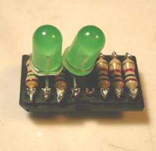
I have found that with most standard parts you can just shove them into the wire wrap socket directly. Like this:
They stay in pretty well but I advise against taking them on a airplane or bus trip.
You can get trimpots with the three terminals inline on 0.1” centers. They are generally multiturn pots like the 3296W. You have to turn them a lot but that’s ok for a wire wrap prototype.
However, there is a caveat for resistors. While there is a standard for the diameter of the leads for 1/4 Watt resistors, the leads on the resistors I get from China (via eBay) are thinner and don’t make good contact in a socket.
From: http://www.resistorguide.com/resistor-sizes-and-packages/#Axial_resistor_size
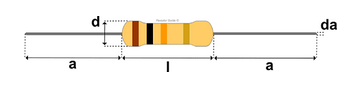
|
Power rating |
Body length (l) |
Body diameter (d) |
Lead length (a) |
Lead diameter (da) |
|
Watt |
mm |
mm |
mm |
mm |
|
1/8 (0.125) |
3.0 ± 0.3 |
1.8 ± 0.3 |
28 ± 3 |
0.45 ± 0.05 |
|
1/4 (0.25) |
6.5 ± 0.5 |
2.5 ± 0.3 |
28 ± 3 |
0.6 ± 0.05 |
|
1/2 (0.5) |
8.5 ± 0.5 |
3.2 ± 0.3 |
28 ± 3 |
0.6 ± 0.05 |
|
1 |
11 ± 1 |
5 ± 0.5 |
28 ± 3 |
0.8 ± 0.05 |
They reference JEDEC : JEP95 – standardized component outlines
but it is behind a paywall.
Here is a comparison of two 100K 1/4W resistors. The bottom one is from China. If you look at the ends of the leads on the left the difference is more obvious
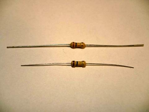
I also find the color bands on Chinese resistors faded and difficult to discern so when I get them I measure a few to make sure they are the correct value and then I put them in a small plastic zipper bag with 4 mil thickness. Then I label the bag. (If the bag is thinner than 4 mils the ends of loose resistors can easily poke through it.)
The Chinese resistors work fine as resistors when they are stuffed and soldered on a PC Board so I maintain a small stock of resistors with standard diameter leads to use for wire wrap prototypes.
And once you are satisfied with your wire wrap prototype make it into a PC Board.
Part 5 - DipTrace
The software that I use is DipTrace (https://diptrace.com/) They offer a free version that is fully functional limited only by the number of pins in the design (300 pins). I am not an expert but I have learned a few things that may make using it easier for you. I will post several projects with schematics and board files that you can modify or just use as is. I will include the Gerber files so if you like my design you can order the boards with them. Note that I use only through-hole devices. I do not do Surface Mount, known as Surface Mount Technology (SMT) or Surface Mount Devices (SMD). And I am doing only two-layer boards. This is not a complete tutorial. It assumes you have some familiarity with DipTrace or can become familiar with it without too much trouble.
First download and install DipTrace. The versions of Windows that I have used it in are: Windows Vista-64, Windows 7, and Windows 10.
Where to start?
The four parts of DipTrace are: Schematic, PCB Layout, Component Editor, and Pattern Editor.
You use Schematic to draw your Schematic and PCB Layout to design your PC Board. So far so good.
A. Creating Your Own Patterns (Shapes)
A. DipTrace comes with a large number of predefined parts but the one you want might not be one of them. Creating your own part can be very confusing. Although I am able to create my own parts I am still not completely sure how I do it. But here goes.
The Pattern Editor creates or edits the Shape on the PC Board. I think Shape is more descriptive than Pattern so that is what I will mostly use. Remember that Shape = Pattern. The Shape consists of the holes, the pads that will be in the copper, and graphics that will be on the silkscreen. An example of a Shape is a DIP20.
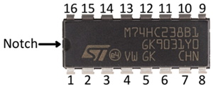
The square pad is pin 1. That will be pin 1 of an actual integrated circuit when the notch (or sometimes a dimple) in the IC corresponds to the notch in the shape. In addition the convention is that when you can read the number on the IC (rightside up) the notch (or dimple) is to the left. This is an example of a 16-pin IC.
DipTrace has shapes for lots of parts like all of the DIPs, various capacitors, resistors, switches, etc.
Here is a shape for a capacitor with 0.1” lead spacing.

Here is a shape for a capacitor with 0.2” lead spacing.

Here is a 1/4 Watt resistor (spacing is 0.4”):

Here is an 1/8 Watt resistor (spacing is 0.3”):

However, DipTrace doesn’t have everything. I created this shape for the 16x2 LCD panel that I use. (It is not to scale here.)
You create a Shape by placing pads. You specify:
1. Surface or Through-Hole. (As I said I only do Through-Hole.)
2. The shape of the pad. A square pad is used for pin 1 of the device. The others should be round. (For my LCD panel I made them all round.)
3. The size of the pad. For standard DIPs the pads (both round and square) are 0.059” (Height and Width) with a hole of 0.035”. This allows you to run a trace between two pins that are 0.1” apart. If it is a large part (like a large electrolytic capacitor) you might want to use a larger pad to better anchor the part to the board. If it is a large electrolytic capacitor the leads will be much farther than 0.1” apart so you can use a larger pad.
4. Each pad needs to have a pad number so it can be connected on the Schematic (and then the PC Board).
Then you put a graphic on the board even if it is only a box. Objects > Place Shape. Otherwise you will have pads with no indication that something goes there. The graphic on the silkscreen will be shown in green, like this:

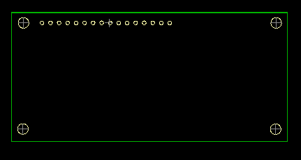
If required you can also place mounting holes. When you do that try to pick a standard size drill bit. That goes for pads too. If you don’t the fabricator will have to do it for you. For a chart of standard drill sizes click here. For my LCD Panel I used 0.125” (1/8”) mounting holes. I also use that size for the mounting holes at the corners of my boards. This size is perfect for using M3 (metric) screws. I use nylon screws and standoffs. I see no reason to tempt fate by using metal which can short things out. Note that mounting holes are not plated so you will get a hole the size of the drill bit. The holes in pads are plated so the hole will be slightly smaller than the drill size.
And make the holes round. If you make a slot it will have to be milled. I expect that will cost more because it requires an extra step.
Important.
When you are specifying holes do not put them too close together. If you do, when the drill is drilling the second hole the drill bit will wander into the first hole, bending the drill bit and breaking it. Fabricators don’t like that.
Once you create a shape you cannot save it to one of DipTrace’s predefined libraries. You have to save it to your own. I am still not really clear where it ends up but I select Pattern > Move to Another Library > User Patterns.
Important.
By default everything has to be on the Grid and by default the Grid is 0.05”. And everything means everything. Pads, holes, labels, and graphics. But not everything wants to be on the Grid. This became apparent when I created the Shape for the 16x2 LCD panel. Sure, when you stuff the board with the actual part you can probably force it to fit but that sucks.
Fortunately, DipTrace allows you to Turn the Grid Off.
You do this by selecting View and then Grid (F11). Clicking on it turns the Grid on and off.
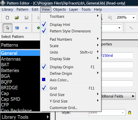
I think having it under the View tab is misleading since it does more than select whether you just see the Grid. It turns the Grid on and off for everything. But now that you know where it is and what it does, it doesn’t matter where it is.
And BTW, this same function applies to Schematic and PCB Layout. In Schematic when you turn off the Grid you can precisely position parts, wires, and labels. In PCB Layout when you turn off the Grid you can precisely position parts, holes, labels, and traces. In Schematic and in PCB Layout you can select a component, press F10 and move the component labels to wherever you want. If you press R while you are dragging a label the label will rotate but you have to be dragging the label for it to work.
I will observe that when you turn off the Grid you are not actually turning off a grid at all. This is a digital system and there is a limit to the resolution. But with the Grid off, the resolution is very fine.
In the Real World you also cannot turn off the Grid. There is the Planck Distance and the Planck Time. The Planck Distance is the smallest distance that an object can move, about 1.6 x 10⁻³⁵ m. The Planck Time is the smallest increment of time and is the time it takes a photon traveling at the speed of light to cross the Planck Distance. The Planck Time is about 10-43 seconds. That is the smallest increment of time when anything can happen. Perhaps we are a simulation running in someone’s computer. Think of the STNG episode “Ship in a Bottle” that ends with Moriarity and Countess Bartholomew being put in a small self-contained box running a holodeck simulation of the entire Universe. And then being put on a shelf and forgotten.
B. Creating Your Own Components
Ok, the Shape consists of the holes, the pads that will be in the copper, and the graphics that will be on the silkscreen. Now we want an actual component that will appear on the schematic and that we can connect to other parts.
That is done in Component Editor.
In Component Editor you define the graphics that will appear on the Schematic. That includes the component pins with labels and pin numbers. Then you tie it to a Shape. That is so the pin numbers of the component in the schematic will be tied to the pin numbers on the PC Board.
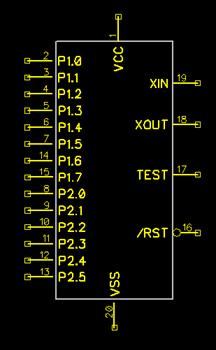
For example, I wanted to do my own MSP430G2xxx microcontroller because I didn’t like the predefined ones.
First I defined the pins with labels and pin numbers.
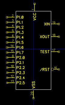
Then I tied it to a DIP20 Shape (Pattern).
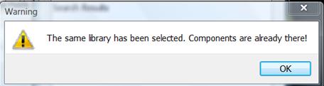
I called my component “myMSP430G2xxx”.
I was already in “User Components” so when I tried to copy it there
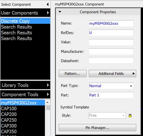
it said
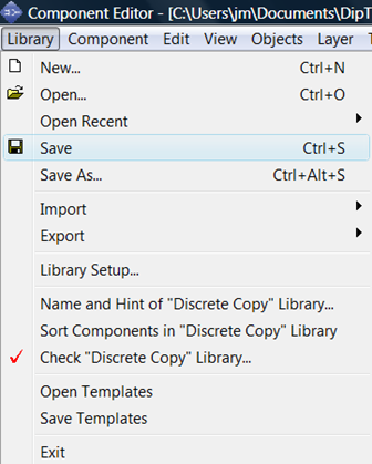
This is important. There is one more critical step. If you leave it out your work will be lost. Go to Library and click Save.
Then, in Schematic, do a search for “myMSP430G2xxx” in “All Libraries” and it will show up in the schematic.
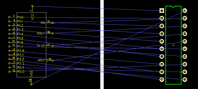
If you select the part and click on “Attached Pattern”
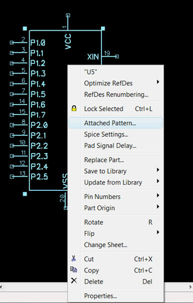
you will see that it is indeed connected to a DIP20.
Note that when I created the part in Components I did not add the label “MSP430G2xxx”.
If I had I would not be able to change it on the schematic.
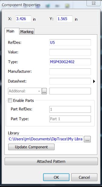
This part is a family of parts (like “MSP430G2402”) so I want to decide which one when I am doing the schematic. You do that in “Properties”.
Another important thing.
When you put a component in a schematic the schematic file saves all of the information about the component including the Pattern (Shape).
When you want to use it again all you have to do is a copy-and-paste it to another schematic.
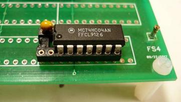
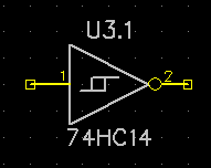
I am posting the schematic file of my MSP430G2xxx along with my 74HC14. The 74HC14 is an inverter with a Schmitt trigger input but the pre-defined 74HC14 DIP does not have the symbol that indicates a Schmitt trigger input.
I have also added a 74HC132 (with the Schmitt Trigger symbol that I seem to have reversed) and the popular 16x2 LCD. For this schematic file click here. If your system does not automatically use DipTrace Schematic to open it then download it to an appropriate folder and then open it.
Some components, like the 74HC14, have several parts. It has six inverters. You can design it so they are all in the same schematic symbol like this. (They put the Schmitt trigger symbol on this part but not the version with individual parts.)
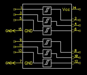
I generally find that inconvenient. I will probably be using inverters in different circuits so I want them separate.
When you start creating a component (in Component Editor) the bottom of the screen will show:
Create the first part of the component.
Then right-click on Part 1.
Select Add.
Now create the second part of your component. And so on.
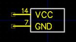
My 74HC14 actually has seven parts. The seventh part is VCC and Ground.
Which is this:
C. Drawing The Schematic
Now you can draw your schematic using DipTrace’s predefined parts and your own.
When you are selecting a component there is something that might not be obvious because it is on the bottom on the screen. This is when the component has several parts, like my 74HC14.
You can have it bring up all of the parts of the component:
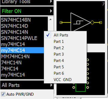
(Right-click on “All Parts”)
or just one of the parts:
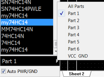
Right-click on “Part 1” (on the left) to select “All Parts” again.
You will eventually have to put all of the parts on the schematic so you might as well put all of them in at the same time.
The reason you have to put all of the parts of a component on the schematic is because you must not leave any inputs floating. Otherwise they will be in an indeterminate state. In CMOS you can connect them either to Ground or VCC. In a completely unused gate (as in a 74HC14) it doesn’t matter which one. If the state of the input does matter (like a 74HC00) connect it appropriately.
If you are using TTL or LSTTL an input that is grounded will draw a small current. If you are using LSTTL and the state doesn’t matter, connect it to VCC. But if you are using actual TTL (which is unlikely) if the state doesn’t matter pull it high to VCC through a pullup resistor.
At Atari we used pullup resistors (generally 1K) even with LSTTL. You can pull up a large number of unused inputs to a single pullup resistor. One of the reasons for doing this was so that when we were bringing up a board, if we shorted out two adjacent pins with a ‘scope probe we would not be shorting +5V to a pin that didn’t want +5V on it. Like an output. (This also applied to technicians in the field repairing a game.)
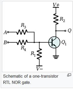
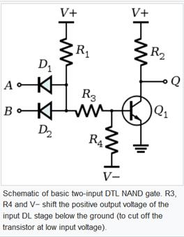
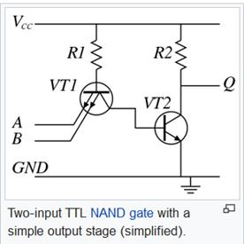
There was probably another reason, an historical reason, going back to the days of the original TTL. TTL stands for Transistor-Transistor Logic. It replaced DTL (Diode-Transistor Logic, which replaced RTL (Resistor-Transistor Logic) and TTL was replaced by LSTTL (Low-Power Schottky TTL).
For historical reference (there were other logic families but these were the main ones):
RTL (Resistor-Transistor-Logic): https://en.wikipedia.org/wiki/Resistor%E2%80%93transistor_logic
DTL (Diode-Transistor-Logic): https://en.wikipedia.org/wiki/Diode%E2%80%93transistor_logic
TTL (Transistor-Transistor-Logic): https://en.wikipedia.org/wiki/Transistor%E2%80%93transistor_logic
LSTTL (Low Power-Schottky-Transistor-Transistor-Logic): http://www.nutsvolts.com/magazine/article/understanding_digital_logic_ics_part_2

NMOS (N-Channel-Metal-Oxide-Semiconductor): https://en.wikipedia.org/wiki/NMOS_logic
You can see that when the output is low you are drawing current through a resistor. It is a small amount of current but it adds up when you have a few thousand gates.
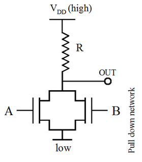
And now there is CMOS (Complementary-Metal-Oxide-Semiconductor): https://www.allaboutcircuits.com/textbook/digital/chpt-3/cmos-gate-circuitry/
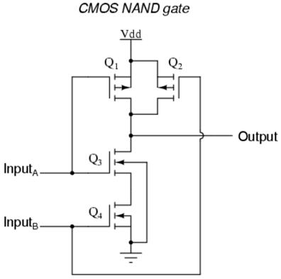
No resisters. Most of the current is drawn when you are switching states.
But in the days of plain TTL you were not supposed to pull up unused inputs directly to VCC. This is from my ancient copy of the TTL Data Book for Design Engineers, Second Edition, Texas Instruments, 1976.
|
unused inputs of positive-AND/NAND gates For optimum switching times and minimum noise susceptibility, unused inputs of AND or NAND gates should be maintained at a voltage greater than VOH min (see tables of electrical characteristics), but not to exceed the absolute maximum rating. This eliminates the distributed capacitance associated with the floating input, bond wire, and package lead, and ensures that no degradation will occur in the propagation delay times. Some possible ways of handling unused inputs are:
a. Connect unused inputs to an independent supply voltage. Preferably, this voltage should be between VOH min and 4.5 V. Series 54LS/74LS devices with diode inputs may be connected directly to VCC.
b. Connect unused inputs to a used input if maximum drive capability of the driving output will not be exceeded. Each additional input presents a full load to the driving output at a high-level voltage but adds no loading at a low-level voltage.
c. Connect unused inputs to VCC through a 1-kΩ [Ohm] resistor so that if a transient that exceeds the input maximum rating should occur, the impedance will be high enough to protect the input. One to 25 unused inputs may be connected to each 1KΩ [Ohm] resistor. Series 54LS/74LS devices with diode inputs may be connected directly to VCC.
d. Connect unused inputs to any fixed-high-level compatible output such as the output of an inverter or NAND gate that has its input(s) grounded. Maximum high-level drive capability of the output should not be exceeded.
|
For the scan of the page click here.
CMOS is a lot easier. Connect unused inputs either to Ground or VCC and be careful when you probe the pins.
Important
In Schematic it is possible for a wire to look like it is connected to a terminal (or another wire) but it isn’t.
If you use Verification > Electrical Rule Check (ERC) it will usually tell you.
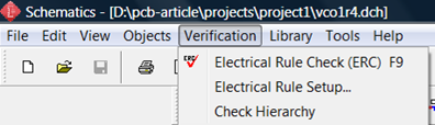
If it isn’t connected in the schematic it won’t be connected on the PC Board.
D. Designing the PC Board - PCB Layout
We have covered creating patterns/shapes (if necessary), creating components (if necessary), and making a schematic (definitely necessary). And we know that we can turn the Grid off so we can put things where we want them to be. Now all we have to do is design the PC Board.
Here is the schematic: vco1r4.dch DipTraceSchematic-vco1r4.pdf
It is for a Voltage Controlled Audio Oscillator using LM13700s. The control voltage can be either external (0-5V) or internal from a trimpot (or a Real Pot can be used instead). The distortion level is about 0.4%. It has three outputs: Line Level, Microphone Level, and Headphones (or an 8 Ohm speaker).
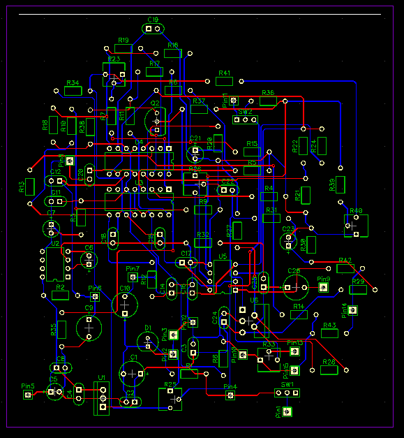
We will start by having Schematic convert it to a PCB. It will place the components on a board in no particular arrangement,
This is the result:
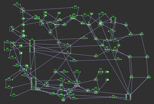
Here are the files ; ex1_1.dip DipTracePCB-ex1_1.pdf
Then there are some choices:
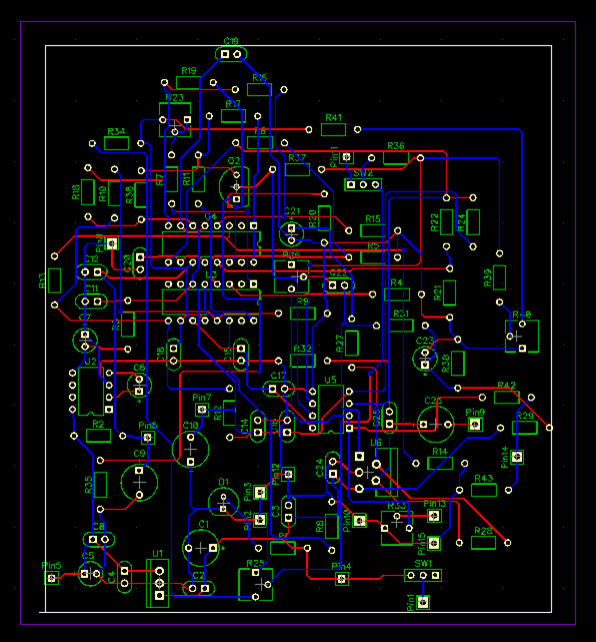
Method 1: Have PCB Layout (“the Software”) place the parts and run the traces. Then you create a ground plane on the bottom. I do a ground plane because ground is always important. If there is noise in the ground to an analog part it will produce a noisy output signal. Noise in a digital part may change the threshold of a digital input so that logic ‘0’ may end up as a logic ‘1’ (or the opposite). Today’s digital parts are generally low power so you probably won’t have any appreciable voltage drop in the ground traces but today’s digital parts also generally have fast rise and fall times which can cause ringing in thin traces. Now add grounds that are daisy chained (from one part to another). So I make a ground plane. And I put it on the bottom layer because that seems to be the best place for it.
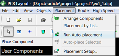
So let’s run autoplacement.
This is the result.
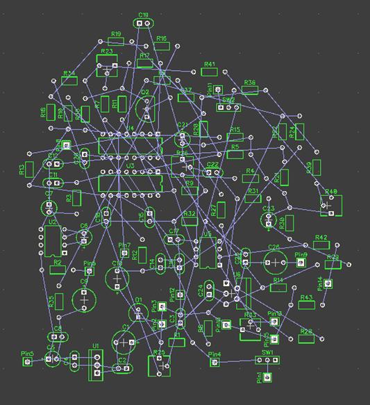
Here are the files: ex1_2.dip DipTracePCB-ex1_2.pdf
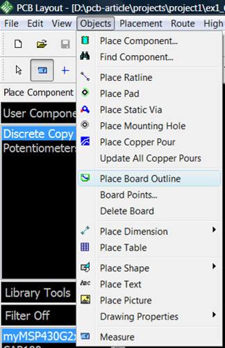
We need to set the size of the board with the board outline:
This is the result.
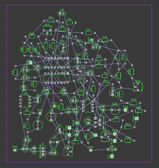
Here are the files: ex1_3.dip DipTracePCB-ex1_3.pdf
The board is 4.55” x 4.95” = 115.6 mm x 125.8 mm. (I like rectangular boards.)
Now we will run the autorouter.
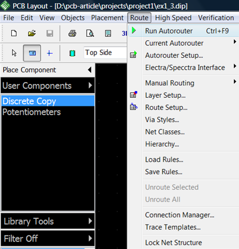
This is the result.
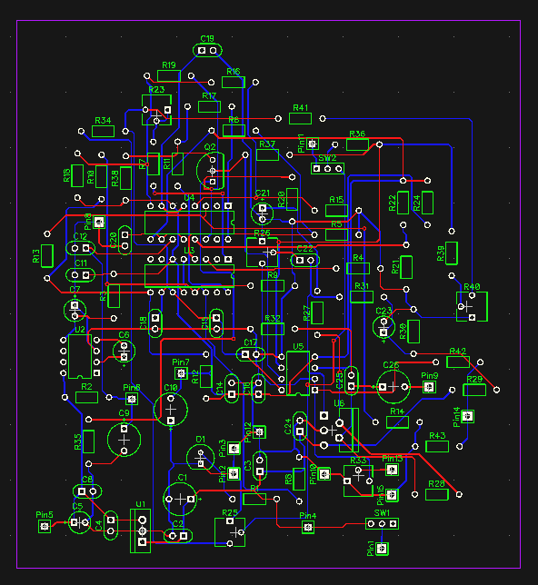
Here are the files: ex1_4.dip DipTracePCB-ex1_4-T.pdf DipTracePCB-ex1_4-B.pdf
Ground Planes
I am going to add a ground plane on the bottom. You have to make sure to specify the layer.
The ground plane is a copper pour.
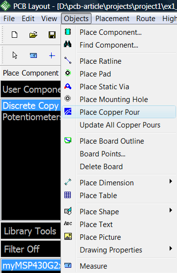
You set the boundaries by drawing lines. The copper pour doesn’t have to be rectangular.
Mine is.
You have to tell it what to connect the copper pour to. Since this is a ground plane we will connect it to ground.
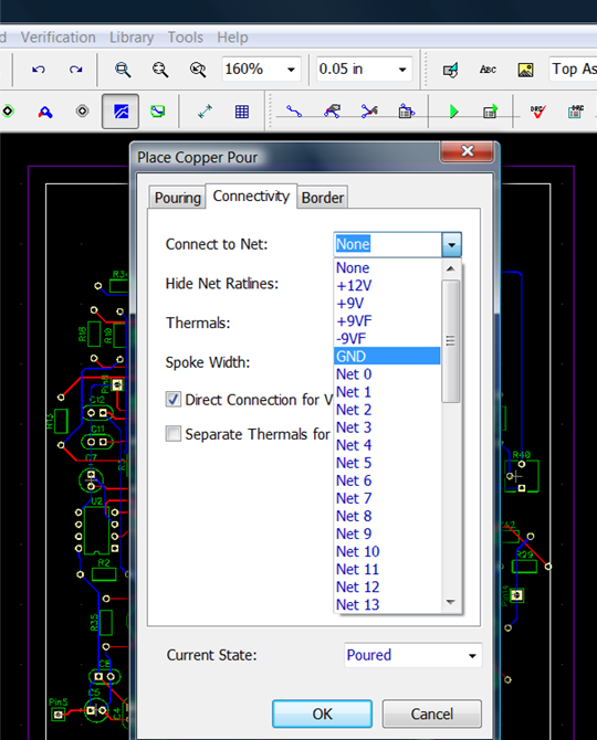
If all you have in the list are Net numbers you should go back to Schematic, find the Ground net, name it GND, and save the file. Then renew the PCB with the schematic.
This is the result of the copper pour.
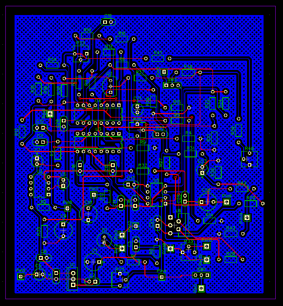
If you look closely you will see that there are many areas of the ground plane that are isolated from each other.
Here are the files: ex1_5.dip DipTracePCB-ex1_5-T.pdf DipTracePCB-ex1_5-B.pdf
Would this board work?
Probably.
But:
1. It is larger than 100mm x 100mm. If you have the board fabricated in China it is remarkably inexpensive if it is no larger than 100mm x 100mm. Generally, for $5 you get 10 boards. If it is larger than that it costs a lot more. (But it is still less than what it would cost from a fabricator in North America.)
2. It’s ugly.
Method 2: I placed the components and used the auto-router. Then I added the ground plane.
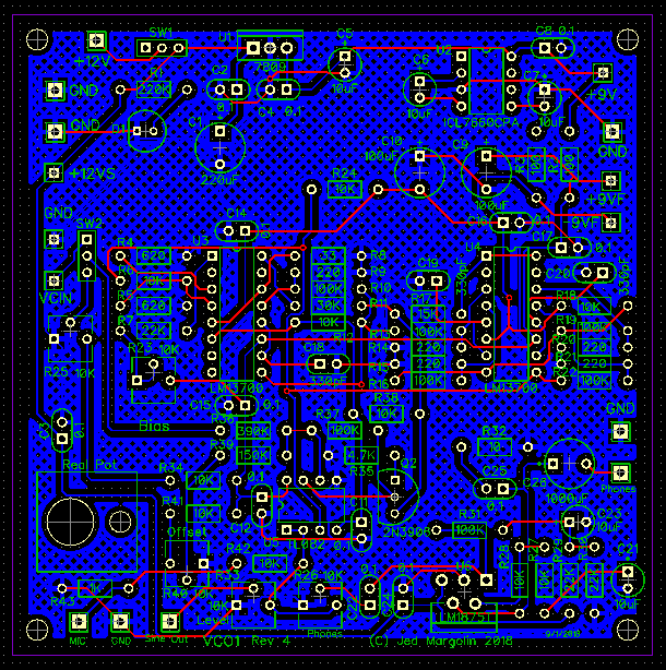
The board is 3.85” x 3.85” = 97.8 mm x 97.8 mm. The ground plane is not too bad but is not as good as I would like. I suppose I am a control freak when it comes to my PC Boards.
Notice that I added holes for a Real Pot. To use the Real Pot instead of the TrimPot R25 you don’t stuff R25 and instead you connect the Real Pot to the R15 pads with wires.
Here are the files: ex1_6.dip DipTracePCB-ex1_6-T.pdf DipTracePCB-ex1_6-B.pdf
Method 3: I placed the components and routed all of the traces myself. Then I added the ground plane.
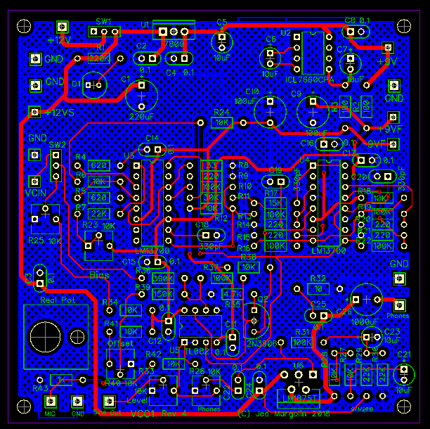
Here are the files: vco1r4.dip DipTracePCB-vco1r4-T.pdf DipTracePCB-vco1r4-B.pdf
Notice that I used thicker traces for Power and the headphone/speaker output. It probably isn’t necessary but it doesn’t cost anything. Also notice that this board is Revision 4. It took me that many times to be satisfied with it.
The board works really well.
This is important.
When you use a Ground Plane (or any copper pour) you should connect the pads to it using a thermal relief pad.
I specify:
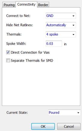
The electrical impedance that it adds is miniscule but the thermal resistance is substantial. Without it when you solder a wire to the pad you will have to heat up the entire surrounding copper.
Also, notice that when I do a cooper pour I do not use a solid pattern. I use a cross hatch. It works as well as solid copper.
The reason I do this goes back to my days at Atari/Atari Games. The way our venders made our game boards was to solder plate the board before putting on the solder mask. When the board was wave-soldered the solder plating reflowed, and with large copper areas (with all that heat energy) it would make bubbles in the solder mask. This was a real problem with my ARII (Audio/Regulator) Board used in games like BattleZone, Star Wars, etc) because the board had large areas of just Ground. The way I dealt with this was to specify “Solder Mask Over Bare Copper” so the boards were not solder plated. (Through holes were still plated since they were done first.) However, since the exposed pads were not solder-plated the boards had to be used before the copper could oxidize. That was not a problem for us. We bought only the number of boards needed for the next production run (and a few spares) and made all of them.
Using a crosshatch pattern reduces the effect of reflowing the solder plating during wave soldering but I am not wave-soldering my boards. And I don’t know if this is still relevant. The fabricators that I have used recently appear to put the solder mask on before they plate it so only the exposed areas get plated.
But these are the parameters I use:
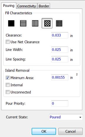
The use of a crosshatch pattern instead of a solid copper pour has been the subject of discussion for the past several years. The current opinions are:
1. If it is a large board and you are wave soldering it, and you have a large solid copper pour on one side and only a few traces on the other side, the different amount of heat absorbed by the two sides of the board can warp the board. Using a crosshatch reduces the amount of copper and therefore reduces the chances of warping the board.
2. If the board is a microwave circuit the crosshatch copper pour will allow you to control the circuit impedances better.
3. If you are going to solder directly to the copper pour (such as when it is a ground plane) it will be easier if it is a crosshatch. This is directly relevant to the two prototype boards I will be posting later.
4. This was a good idea “back in the day” but with modern PCB manufacturing it is totally unnecessary.
5. It doesn’t matter and some people think the crosshatch looks better than the solid pattern.
After you have put down a ground plane (copper pour) and you want to remove it this is what you do. I will use as an example a crystal oscillator. For the board file click here.
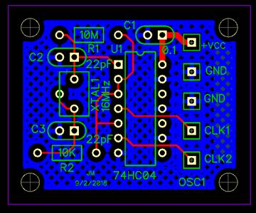
Select the layer where the copper pour lives. On this board it is the bottom.
Notice that the top traces (in red) are now behind the bottom layer (in blue).
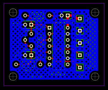
Put the cursor on one of the borders of the copper pour. The border will be highlighted in pink.
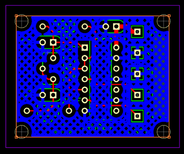
Click on it. The pink borders go away and are replaced by pink squares at the corners.
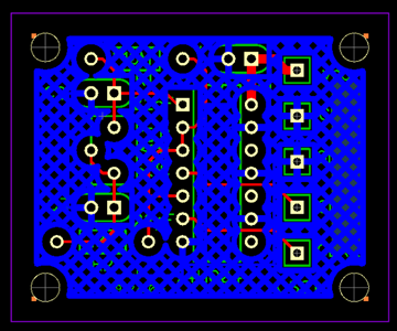
Press Delete. And the copper pour is gone.
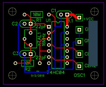
Making a Void in a Solder Mask
Notice the grey rectangle on the right side of the board. That is where I removed a section of the bottom solder mask. Since it was over the ground plane it would have left that area of ground plane exposed. If I use the oscillator in a circuit where I need a better ground connection than I can get with the two Ground pins I can use copper foil tape to bond the oscillator ground to the ground of the circuit I am using it with.
This is how you make a void in the solder mask.
1. Start with the board with the intact solder mask. For the board file click here.
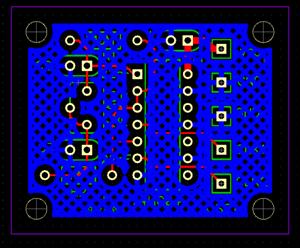
Make sure you select Bottom Mask and Bottom Layer.
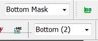
Select Objects > Place Shape > Filled Rectangle
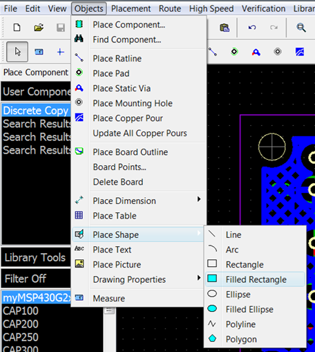
Draw the rectangle where you want to remove the bottom mask. The other filled shapes will also work. They have to be filled shapes or you will only get lines removed in the solder mask. (Since the line will be a gap in the solder mask and not in a copper layer such as a copper pour I can’t think of a reason for wanting to do that.)
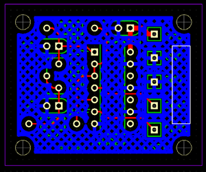
Release the mouse button.
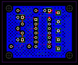
For the board file click here.
If you do File > Export > Gerber
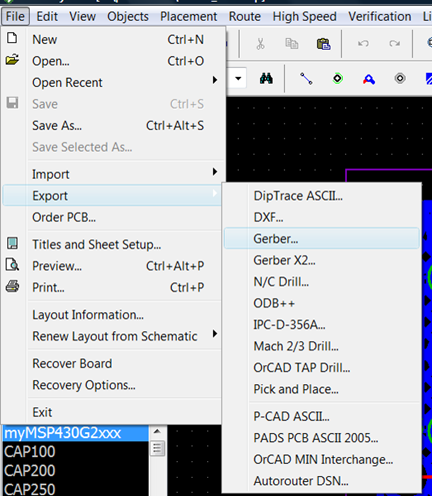
and then Bottom Mask and the Preview button (below the box)
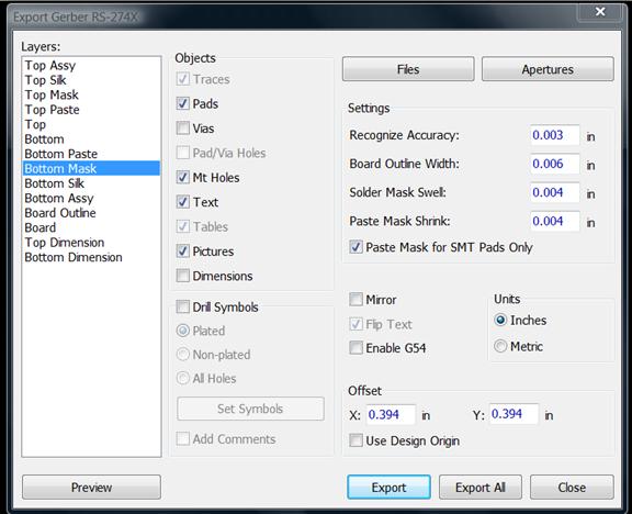
you are shown the bottom mask. Success!
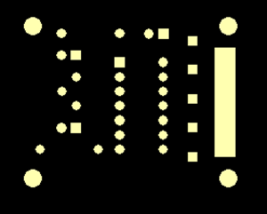
You can also select any of the other layers to see and you can select more than one layer with the Ctrl key but they will all be shown in the same color.
This is the board.
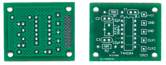
Some Other Important Things
1. Run Verification periodically.
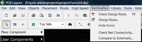
Check Design Rules tells you if you have shorted out some traces. It only does this for traces that you have run. It does not tell you if you have left out some traces.
Check Net Connectivity tell you if you have run all the traces.
Compare to Schematic tells you if your board matches the schematic.
2. When you are putting a label on the board make sure you are putting it on the Top Silkscreen.
Although, if you really want, you can put a label in a copper layer.
If you put it on a layer that isn’t used, you won’t have a label on the board.
3. One More Thing - Component Labels.
When you place the components on the board they have only the reference designations, not the component values (or type or name), things that I want on my board.
Adding it to each component one at a time is a PIA. Fortunately you don’t have to do that.
With resistors I put the resistor value in the middle of the part. With capacitors there generally isn’t room. With terminal pins, I don’t want even the reference designation on the board. I will add my own label to say what the signal is.
I will start with resistors.
After you place the parts on the board move all of the resistors to the same area.
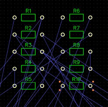
Draw a border around them.
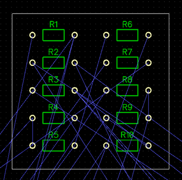
When you release the mouse button the resistors will all be surrounded by pink squares.
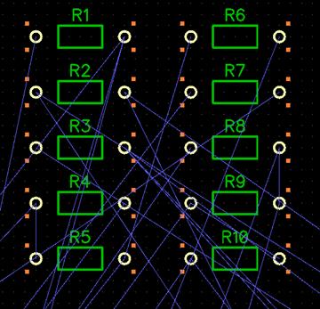
Use the mouse to select one of the resistors.
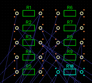
Right-click and select Properties and then Markings.
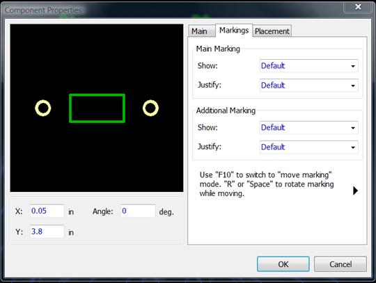
The Main Marking defaults already show the Reference Designation.
For Additional Marking I select Value and Center.
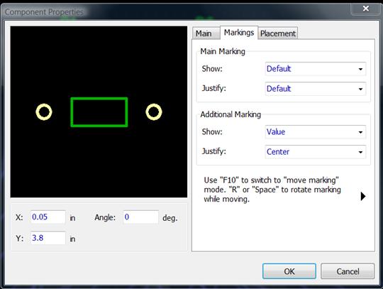
Then OK.
This puts the resistor values in the centers of all of the resistors that we have selected. All at once.
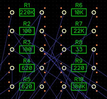
The same works for capacitors. Put them together, draw the box around them, and select one capacitor. Since there usually isn’t room for the values inside the capacitors I’ll put them on the bottom for now.
. 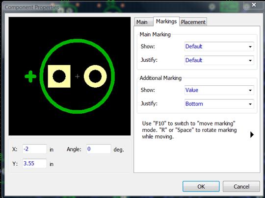
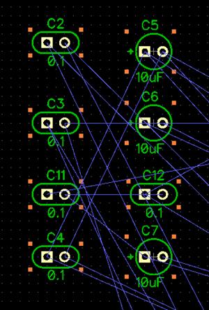
For the test pins I set it to none. I will label the pin signals myself.
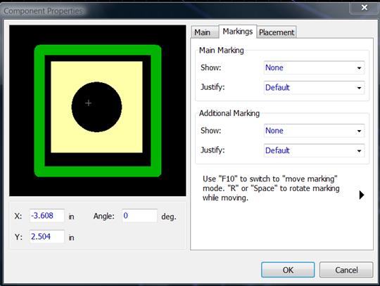
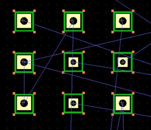
Then move the parts where you want them (or use auto-placement) and design your board.
(Notice that there are two types of pins. I designed my own with a larger hole and pad.)
Part 6 - More Useful Software and Some Hardware (for the audio projects)
A. GerberLogix - Gerber File Viewer
It is useful to be able to view Gerber files that is separate from the built-in viewer of DipTrace. For years I used GCPrevue (starting with the DOS version) even though I only used a small part of it. It was free. Now it isn’t. Now I use GerberLogix. This does what I need, which is to view Gerber files. The program runs in place, meaning that it does not install anything on your computer. You just run the program. And it is free. And it is here: https://www.easylogix.de/products_detail.php?prog_id=1 Download it to wherever you want it to live. I have mine in the DipTrace folder because I always know where that is. You can select the zipped board file and it will unzip it and show you the layers. You can select which layer to look at and you can look at all of the layers at once in different colors. Very nice.
B. CutePDF - for making PDFs
CutePDF appears to your system as a printer. You "print" to it, and it converts the document to a PDF document. The download page for the free version: http://www.cutepdf.com/Products/CutePDF/writer.asp. It requires PS2PDF converter such as Ghostscript (recommended). The link is on the Download page.
Here is a simplified explanation of PDF.
PDF is a descendant of PostScript. PostScript is used in desktop publishing and was the Killer App for the Apple Macintosh.
Here is an article on PDF on Wikipedia: http://en.wikipedia.org/wiki/Portable_Document_Format.
PDF allows you to have fonted text (with an embedded font) and graphic images. An embedded font means the font is included in the file. It does not get the font from the Operating System.
When you start from a word processor (like Microsoft Word) and create a PDF file from it with CutePDF, your text goes into the PDF file as fonted text. Pictures go in as pictures.
But if you scan a document in a scanner, everything is a graphic image (a picture).
Fonted text takes up a great deal less file space than images (pictures). It also allows the PDF file to be text searchable. And, you can usually copy-and-paste text from the PDF file to another program.
You cannot search text that is in a picture. You can copy-and-paste pictures, but you cannot edit the text in pictures other than with picture editing software like PhotoShop.
Example:
Here is my article The Road to the Transistor as a Microsoft Word document: transistor.doc (62 K Bytes). I have now updated the links and made it an html file. Click here.
Here it is as a PDF file created using CutePDF (more about CutePDF later): Microsoft Word - transistor.pdf (73 KBytes)
I printed the article from Microsoft Word and scanned it using a scanner at 300 dpi: Scanned - transistor.pdf (547 KBytes)
And here I "printed" it from Microsoft Word into Paperport 11SE and saved it as a PDF file: PaperPort - transistor.pdf (9.3 MBytes)
This last one is 9.3 MBytes, and it doesn't even look very good.
CutePDF is available as a free program at http://www.cutepdf.com/. (They also have versions that you can pay for.) CutePDF appears to your system as a printer. You "print" to it, and it converts the document to a PDF document. If your document contains fonted text then the PDF created by CutePDF will also have fonted text. The only thing CutePDF doesn’t do is carry over embedded links.
The free version requires a component from Ghostscript: http://www.cutepdf.com/Products/CutePDF/writer.asp
Ghostscript is an extremely useful program that reads almost every PDF file, even when Adobe Reader won't. It also reads Postscript files. Ghostscript allows you to convert PDF files into a wide variety of other formats, such as .bmp and .png files. The reason this is useful is that then you can use the .bmp and .png files with OCR software, such as Omnipage. A tip: when converting a PDF file to .png for OCR, output it as a color image: png256 at 300 dpi. The OCR software will do a better job than if you make a simple B/W file.
Ghostscript is worth getting. It is also free: http://pages.cs.wisc.edu/~ghost/
Or, you can buy software from Adobe (http://www.adobe.com/products/acrobat/) as well as from several other companies.
There are two other things you might want to do with PDF files.
1. You want to number the pages.
If your document comes entirely from a word processor, you can number the pages with the word processor.
However, if your document has been put together from several sources (like several PDF files) it can be a problem.
There is a really great (and free) program for adding numbering to a PDF file: A-PDF Number, available at http://www.a-pdf.com/number/index.htm (Home page: http://www.a-pdf.com)
You can tell it what page to start at, what number to start with, and where to put the numbering. You can also add a prefix to the number.
2. You might have to merge PDF files that come from different sources.
A-PDF makes a product for this called A-PDF Merger (http://www.a-pdf.com/merger/index.htm) This one costs money but it isn't much, and it is worth it.
A-PDF Merger also allows you to number the pages, like A-PDF Number.
3. You might need to split a PDF file.
One way to do this is to print the pages you want and then scan them. That will convert your nice fonted text to a pure image with a large file size and poor quality.
A-PDF makes a product that separates pages in PDF files called A-Split. http://www.a-pdf.com/split/index.htm. It is also very worthwhile.
I make PDFs of my Schematic and
Board files so I can look at them and print without opening the DipTrace
programs. This is also a good way to archive them. I am not saying that
DipTrace is in any danger of going away. It is because of my experience with
OrCad for DOS which I used in the early 1990s. Even though I still have the
original OrCad program I cannot run it except in a DOS virtual machine running
on my Windows 7 machine. And printing it still requires a printer with a
parallel port. PCs generally don’t have parallel ports any more and my last
printer with a parallel port died a few years ago. I cannot use a USB to
Parallel Port Adapter because raw DOS does not support it. While I was still
able to I printed out all of the schematics I had done with OrCad and then
scanned them. I don’t want to have to do that again with my DipTrace projects.
Again, I do not think DipTrace is going away.
I make a PDF of my schematic in Schematic selecting Print and then choosing:
Then it asks where I want it to go and what I want to name it:
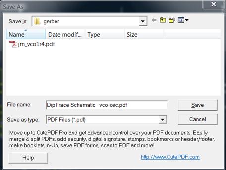 :
:
That is how CutePDF works with everything that you can print.
I make a PDF of my PC Boards by using Print > Preview. This allows me to make separate files for the Top and Bottom. I usually make the PDF with a 200% zoom.
C. ARTA - Audio Measurement and Analysis Software
This ARTA software is an excellent audio spectrum analyzer program that runs on a PC. It does an accurate job reporting Total Harmonic Distortion (THD) and THD+Noise which is what you want. Get it at http://www.artalabs.hr/ and install it.
Several of my projects are for audio. Any periodic waveform can be represented as a series of sines and cosines at its fundamental frequency and at harmonics of its fundamental frequency. No other signals are needed. It is called a Fourier Series. https://en.wikipedia.org/wiki/Fourier_series.
A pure sine wave has energy only at the frequency of the sine wave.
A symmetrical square wave has energy at its fundamental frequency and at odd harmonics (and only odd harmonics). So a 1KHz square wave has energy at 1KHz, 3 KHz, 5 KHz, 7 KHz, etc. As the harmonics go up the amount of energy at each harmonic goes down.
A symmetrical triangle has energy at its fundamental frequency and also at odd harmonics (and only odd harmonics). So a 1KHz triangle wave also has energy at 1KHz, 3 KHz, 5 KHz, 7 KHz, etc. and as the harmonics go up the amount of energy at each harmonic goes down. However, it goes down faster than a square wave does.
Any distortion of a pure sine wave affects the waveform and creates harmonics so one of the important qualities of audio equipment is Total Harmonic Distortion. This can be analyzed either with analog or digital methods. My venerable old HP 331A Distortion Analyzer contains a very sharp analog filter that you tune to the fundamental frequency of the signal you are feeding it. It filters out the signal at that frequency and reports whatever is left. The way you can use it is to feed a low distortion sine wave into a piece of audio equipment such as an amplifier and send the output of the amplifier into the HP331A. After you twiddle the knobs appropriately the HP331A reports the amount of total harmonic distortion (THD). Technically, it reports the amount of THD+Noise. For the HP331A manual click here. If the signal that comes out of the amplifier has more distortion than the signal that went in, it must have been caused by the amplifier. You can also test audio equipment with a spectrum analyzer. Here is The Tektronix Cookbook of Standard Audio Tests. Click here. Although this is an old article (1975) and shows vacuum tube equipment being tested much of it is still relevant. The Tektronix 5L4N is an analog spectrum analyzer. Click here. It is a very selective receiver that is slowly tuned through the frequency band of interest. Because it tunes slowly the results were displayed on a storage oscilloscope (an analog storage oscilloscope). That is why the 5L4N was a plugin module for the Tektronix 5100 series oscilloscope mainframe which was available as a storage ‘scope such as the model 5111.
You can also do it digitally. That is what the ARTA software does. It does a very good spectrum analyzer and can report the amount of THD or THD+Noise (which is what you want).
Getting the ARTA program to display THD+Noise is not intuitive. This is how you do it.
1. Start the program.
2. On the tool bar select Spa
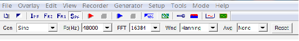
3. Select View > Info > Distortion+Noise
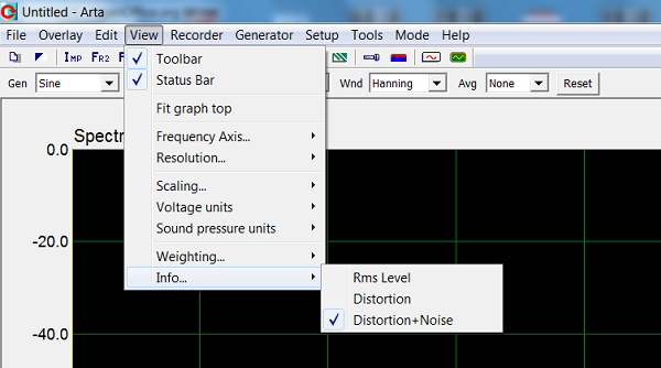
4. Set Gen to External. Otherwise it will use an internal test tone.
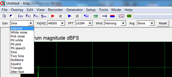
5. Press the Record Button (Red Triangle)
6. To stop recording press the Red square button under Recorder.
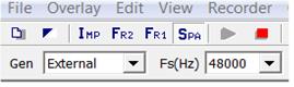
Why would you want to stop it? To save the results.
There are two ways to do that.
1. Use Print Screen to do a screen capture. That puts it into the Windows Paste Buffer. Then you paste it into your favorite word processor.
2. Use the Windows Snipping Tool that comes with all versions of Windows. This allows you to do a screen capture of a box that you make with your mouse (or other pointing device). Do a Windows Search for SnippingTool.exe . In Windows Vista 64 and Windows 7 it is Windows/System32/SnippingTool.exe . Send it to your Desktop (it creates a shortcut) and then drag it to the Toolbar. In Windows 10 type “snip” into the search box. Then you can put it on the task bar. (The less I look at Windows 10 the better.)
Since you will be capturing most of the screen anyway what is the advantage of using the Snipping Tool?
The Snipping Tool allows you to save what you have captured as a file with a choice of several formats: .PNG, .GIF, .JPG, and .MHT.
This is the Triangle wave that my Triangle (and Square) Wave Generator (Project 4) produces.
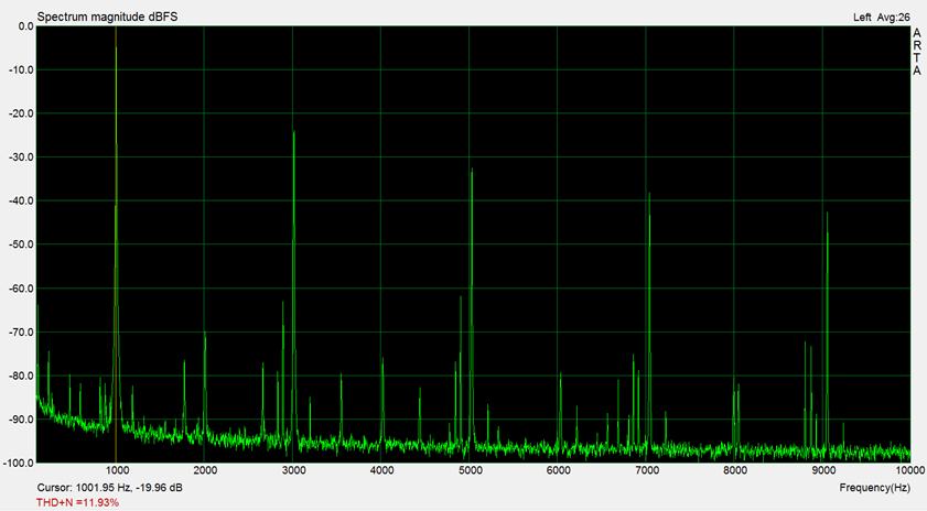
It shows a THD+Noise of 11.93% which is about right for a symmetrical triangle wave. The theoretical value is 12.1%. https://www.vcalc.com/wiki/MichaelBartmess/THD+Triangular+Wave
This is what the square wave output produces:
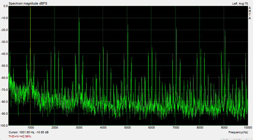
It shows a THD+Noise of 42.98% which is about right for a symmetrical square. The theoretical value is 48.3%. https://www.vcalc.com/wiki/MichaelBartmess/THD+Square+Wave. Mine is lower probably because the edges are not all that sharp.
The reason I made the Triangle (and Square) Wave Generator is because I had been using a different spectrum analyzer program and I did not believe the results for THD+Noise. That program is Visual Analyzer 2011 XE Beta 0.3.2 by Alfredo Accattatis. http://www.sillanumsoft.org/ This is a great program but either it doesn’t do THD properly or I couldn’t figure out how to make it do THD properly.
And this is what my Johnson Counter Sine Wave Generator (Project 3) produces. A sine wave with 0.3% THD+Noise. Not bad for a simple circuit.
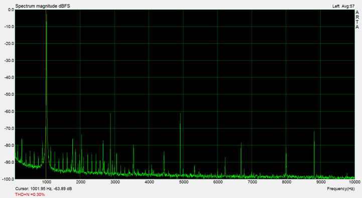
It shows why you have to measure THD+Noise. In a digital system there is going to be digital crap between the harmonics.
D. External Audio Pods For The Audio Projects
Several of the projects are for audio. That is why I am using the ARTA program.
Don’t use on-board audio. It is going to pick up the digital crap on the motherboard. Use an external audio pod.
I am using the Startech ICUSBAUDIOB external audio pod. For the datasheet click here. This is a USB audio pod that has stereo outputs but the input (a microphone-only input) is mono. This is made clear when you look at the datasheet for the Cmedia CM-108AH chip that is uses. But the input is a 16-bit ADC. For this datasheet click here.
When I do the measurements I use a notebook PC and take the extra precaution of running it on its battery during the tests to avoid possible line noise switching crap from the power supply.
If you need an audio pod with stereo inputs I recommend the Behringer U-CONTROL UCA222 USB audio interface. Its two inputs are line level which I consider an advantage for the work I have been doing. With the Startech I have to use a pad to bring the my line levels down to mic level. I did a board for that too (Project 6).
Part 7 - Making the Gerber Files and the Drill File
This may seem complicated but before there was Computer Aided Design the masks for printed circuit boards were made by hand by putting black tape on vellum at 2x or 4x size. It was then photo-reduced for making the PC Board. Aren’t you glad you don’t have to do that?
If you are doing more than one project it is easy to get things mixed up. I am presenting the method I use.
When you install DipTrace it will create several folders under User Name > Documents
Under Projects I make a folder for each project. I also make a folder called Parts where I put the datasheets for some of the parts I use.
When I make a new revision of a board I make a new folder for it. And I try to make the revision number part of the project name. I admit I have not been very consistent in how I do that.
In order to compare your results to mine create a folder named example_osc1-R1. Download and save this file (proj5_jm_osc1-R1.zip) to the folder and unzip it.
Now create a folder named osc1-R1. Under that make two folders: gerber and order.
In the osc1-R1 folder I keep the schematic and board files and the Bill of Materials spreadsheet if I remember to make it. I also keep the PDF files of the schematic and the board.
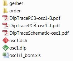
Download and save these files in folder osc1-R1: osc1-r1.dch and osc1-r1.dip.
When I make the drill and Gerber files they will go in the gerber folder.
In the gerber folder I start with two of my own files: 0osc-r1.doc and 0osc-r1_copy.bat . (Since 0osc-r1_copy.bat is a command file, in order to read it open it with Edit.) Download and save these files in subfolder gerber: 0osc1-r1.doc and 0osc1-r1_copy.bat
I start these filenames with a zero so they will always be the first files in the folder. When DipTrace makes the drill and Gerber files it is very easy to have them end up in the wrong project. This way you will always be able to check that you are putting them with the correct project.
The file 0osc1-r1.doc contains some basic information about the board. Now the file 0osc1-r1_copy.bat .
When DipTrace makes the drill and Gerber files it names them:
Top.gbr
TopMask.gbr
TopSilk.gbr
Bottom.gbr
BottomMask.gbr
Through.drl
BoardOutline.gbr
Through.drl is the drill file.
BoardOutline.gbr is (no surprise) the outline of the board. That is how the fabricator knows where the sides of the board are.
Since the fabricator may get several thousand orders a day I distinguish my files by putting my initials and project name at the beginning of each one. 0osc1-r1_copy.bat is a command file that copies the DipTrace files and puts my initials and project name on it. This is what 0osc1-r1_copy.bat contains:
rem jm_osc1r1
copy Top.gbr jm_osc1r1_Top.gbr
copy TopMask.gbr jm_os1cr1_TopMask.gbr
copy TopSilk.gbr jm_osc1r1_TopSilk.gbr
copy Bottom.gbr jm_osc1r1_Bottom.gbr
copy BottomMask.gbr jm_osc1r1_BottomMask.gbr
copy Through.drl jm_osc1r1_Through.drl
copy BoardOutline.gbr jm_osc1r1_BoardOutline.gbr
All you do is double click on 0osc1-r1_copy.bat and it runs.
The result is that you will have 8 files starting with jm_. Those are the 7 files used for making the board plus the information file.
I should mention that when DipTrace makes the Gerber files it is capable of making masks that you will not need and the fabricator will not use. Don’t send the fabricator unnecessary files. You can specify which files DipTrace should make but I find it easier to have it make all of them. My command file just uses the ones that are necessary to make the board.
Now let’s have DipTrace make the files.
1. I will assume you have already downloaded and saved the schematic and board files osc-r1.dch and osc-r1.brd .
2. Open osc-r1.brd .
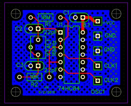
3. Select File > Export > N/C Drill (N/C Drill means Numerically Controlled Drill)
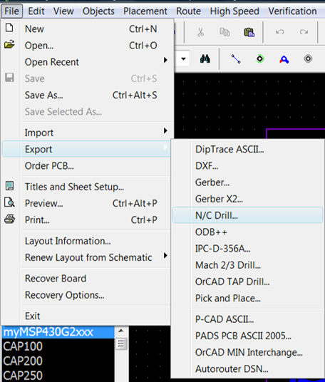
You will get this:
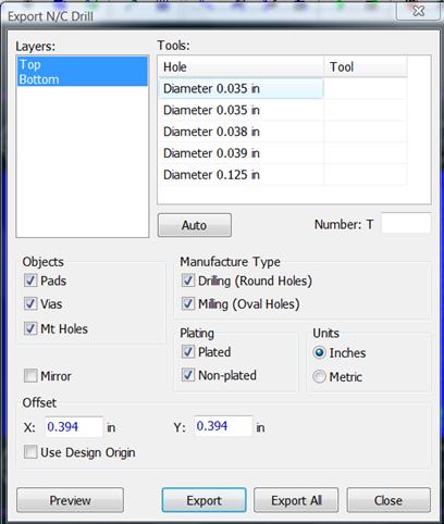
4. Select the button Export All.
It will produce this message:
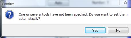
I don’t know why it does that. Just say Yes.
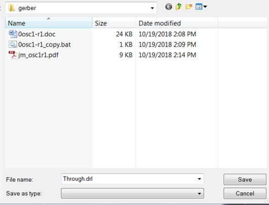
The files we put in the project folder osc1-R1/gerber (0osc1-r1.doc and 0osc1-r1_copy.bat) show us that we are in the right folder. Otherwise we would have to climb up the directory until we figure out where we were and then go back down to it.
5. Click on Save. And then Close.
Good. We have the drill file.
Now the Gerber files.
1. Select File > Export > Gerber
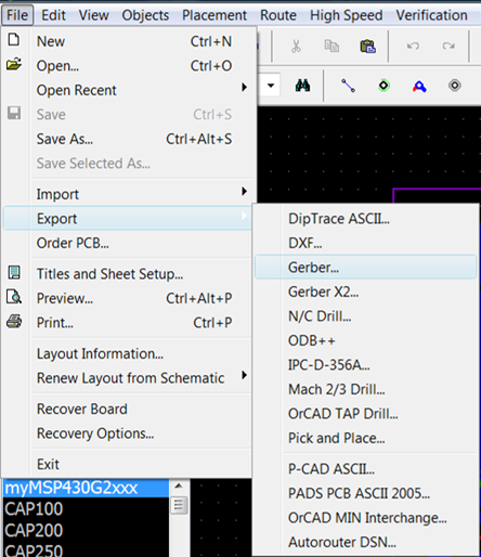
We will get:
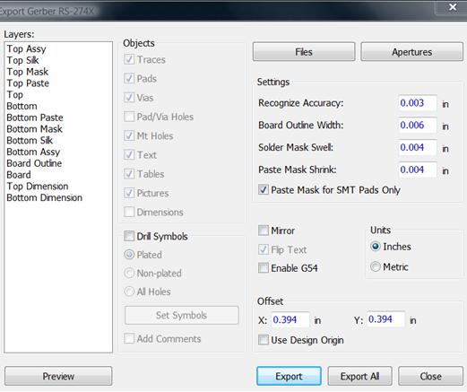
2. Click Export All.
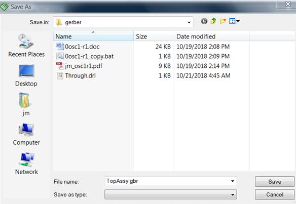
Click Save.
This is the first of 13 files. Keep going and save all of them.
Before you click on Close notice the button on the bottom of the left box that says Preview.
Click on a layer such as Top Silk, then click on Preview and it will show you that layer.
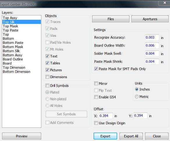
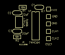
This is the Top layer.
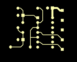
And so on.
This is useful but not a substitute for an independent Gerber File Viewer like GerberLogix .
Now that we have created the layers that we need, double click on the command file 0osc-r1_copy.bat and we should have the 7 files for making the board and the information file.
These will be the only files in the gerber folder that start with jm_ .
The next step is to copy these 8 files to the folder order.
We will put them all in a zip file by selecting all of them, do a right click, and send to Compressed (zipped) Folder.
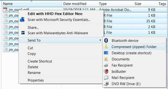 .
.
Make sure the zipped file gets the name you want it to have. I want it to be named jm_oscr1.zip.
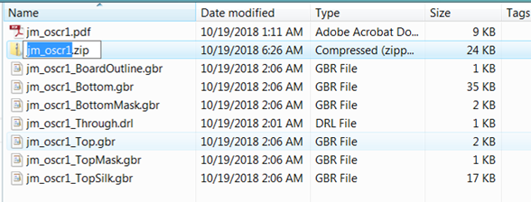
That is the file that contains all of the files needed to make the board plus the information file.
Important. If you make a change to the board and create new files (Gerber, drill, or info) and copy them to the order folder the zipped file will not automatically update itself. You have to delete it and make a new one.
But we are not done.
Create a folder somewhere away from the DipTrace. Call it something like pcb5 which could mean PCB Order #5.
Copy the zipped board file (jm_oscr1.zip) to it.
Now use your Gerber File Viewer (like GerberLogix) to look at the layers and drill file. GerberLogix will unzip the board file for you. If you use a Gerber file viewer that doesn’t do that you will have to unzip the file yourself.
Is this the board you want to order? Is it the right revision of the board you want to order?
Did you remember to put in the ground plane?
Did all of the labels you put on the Silkscreen get put on the Silkscreen?
If you put a Void in the solder mask is the Void there?
Did you notice something in the Top (or Bottom) layers that you want to change? Something you can do better even if the board will work the way it is?
Now is the time to do it, not when you have the board in your hands and you are about to stuff and solder it.
If possible, put it aside for a day or two and then look at it again. You may see something that you hadn’t seen before.
Then when you are ready, choose a fabricator and upload the file from the pcb5 folder (or whatever folder you named it) because that is the board you have checked.
And when you do your own boards use your own initials.
Part 8 - Buying Parts
I try to buy my parts through eBay because they cost less. The best prices are from China. There are U.S. companies on eBay. They charge more but you get the parts faster.
During the past year (2017-2018) I have gotten some bad parts from China. They are parts that I bought from different companies. At least I think they were different companies.
These are the parts: TL062, TL064, TL082, TL084, and ICL7660CPA. With only one exception when I contacted the companies they immediately gave me a full refund and did not want the parts back. When you send parts back to China you have to send it with tracking. The only way to send it with tracking is by Global Priority Mail. Global Priority Mails starts at $49.
The one exception, the company that insisted I send their bad parts back, was a scam artist who wasted my time figuring I would give up. And eBay and PayPal dropped their balls. Since they wasted so much of my time I wrote about it: www.jmargolin.com/ebay/bad_eBay_01.htm .
And I do not buy the above parts from China anymore. I don’t have any problem buying other parts from China.
These are my favorite companies to buy parts from:
Tayda Electronics (https://www.taydaelectronics.com/) Very good prices, shipping costs are reasonable, they take a little longer to ship than the other companies. Tayda is also an eBay seller but buy from their Web site.
Jameco Electronics (https://www.jameco.com) Their prices aren’t great but shipping is reasonable and fast. However if your order is for less than $15 they tack on $5.00 .
Newark Electronics (https://www.newark.com/) Prices are generally high but shipping is very fast. I think they charge too much for shipping, probably because they send things in boxes that are unnecessarily large for the items being shipped.
Digikey (https://www.digikey.com/) Prices are generally high but shipping is very fast. I think they charge too much for shipping, probably because they send things in boxes that are unnecessarily large for the items being shipped.
Mouser (https://www.mouser.com/) Prices are generally high but shipping is very fast. I think they charge too much for shipping, probably because they send things in boxes that are unnecessarily large for the items being shipped.
Part 9 - About Me
I got into ham radio early. I got my Novice license (WV2VEW) in 1961 when I was 11 years old. My mentor was Sidney Goldin, an electrical engineer who lived up the street from me. I got my General when I was 13 and became WA2VEW. I built a bunch of stuff. Since it was the 1960s they all used vacuum tubes. It wasn’t all ham gear. One time I modified an old TV so I could display Lissajous figures. I still find them entertaining. See www.jmargolin.com/mtest/LJfigs.htm . I got my Amateur Extra (still WA2VEW) some time in the middle 1970s. I still have it but I don’t operate much anymore.
I got my BSE(EE) from The University of Michigan in 1972. My area of concentration was Computer, Information, and Control Engineering. My favorite professors were Dr. Lawrence McMahon (electronic circuits) and Dr. Gabriel Weinreich (physics).
When I graduated in 1972 there was a recession and they weren’t hiring many engineers. I got a job at The University of Michigan’s big public radio station (WUOM) as a radio engineer. I was a board operator on the weekends and during the week I did maintenance and built some new equipment. I designed and built some killer RIAA phono preamps. I also designed and built a very nice stereo control room. WUOM was one of the founders of NPR. (That might have been a mistake since NPR has pretty much destroyed public radio in this country.)
At WUOM one of the people I worked with was the famous avant-garde composer George Cacioppo. George worked as a radio engineer because he was afraid that if he taught at the School of Music (which they wanted him to do) it would compromise his art. We had a piano in one of our three cavernous studios. Sometimes, on a break, George would play it. He would tell people that he was de-composing. Another one of my co-workers was a very young Evans Mirageas (an announcer and producer) who went on to become the Artistic Director of the Cincinnati Opera.
At one point I went to visit my Mother in New Jersey. She took me to a huge shopping center where I saw my first video arcade and first video game. I looked at the game and thought, “I can do better than this.”
When I went home to Ann Arbor I started working on it. I eventually quit my job at the radio station to work on it full time. I made it work and did a simple 2D Space War game on it. I filed my first two patent applications which later became U.S. Patent 4,179,124 Electronic Video Game issued December 18, 1979 and U.S. Patent 4,195,293 Random dot generator for raster scan video displays issued March 25, 1980.
While I was waiting for the Patent Office to get to my applications the first Star Wars movie came out (summer 1977). I was blown away. I left the theater thinking, “ I have to do a 3D Space War game.” I had had computer graphics in college and knew how everyone did it. They used homogeneous coordinates which are very computationally intensive. I knew there would be no way to do realtime 3D with homogeneous coordinates. At the time the computer graphics community was doing what I called Pretty Pictures where it would take a few hours (or many many hours) to render one frame. The only people doing realtime 3D graphics were companies like Singer-Link who did $10M flight trainers for the military. I came up with a different way of doing it that was much less computationally intensive but still did the 3D math exactly right. I called it Unit Vector Math for 3D Graphics. My Unit Vector Math is also free of the nasty “axis problem” that Euler function rotations have.
I sent my patent applications around to the various video game companies. No one was interested in them but Atari offered me a job as a hardware engineer in the Coin-Op Division that made the games for the arcades. I took it (1979).
Most of the games I worked on were 3D simulator games. The first one was BattleZone which is considered the first real 3D game. I was nominally the hardware engineer but I mostly I just did the 3D algorithms and the hardware sounds. (The throbbing motor was mine.) After the game came out we were approached by a group of Army colonels who asked us if we would convert it into a trainer to teach the gunners in the new Infantry Fighting Vehicle (later renamed the Bradley Fighting Vehicle) how to properly fire TOW missiles. It was originally called Army BattleZone and then became the Bradley Trainer. This is a good article about it: https://arcadeblogger.com/2016/10/28/bradley-trainer-ataris-top-secret-military-project/
After that I started working on a 3D space war game as Project Engineer and Hardware Engineer. The working title was originally Warp Speed. It became Atari’s Star Wars and was a big success. Then came TomCat (a 3D flying game), and Hard Drivin’ and Race Drivin’ (3D driving games). I still have my Star Wars, TomCat, and Race Drivin’ prototypes. A few years ago I made videos of them: www.jmargolin.com/videos/
At Atari/Atari Games (Coin-Op) the engineers designed the circuits and gave it to the Assembly Group who wire wrapped the prototype boards. The Assembly Group was led by Karen Bjorkquist. Her wire wrap boards were pure art. And they worked, too. Eventually our designs would go to the PCB Design Group who designed the PC Boards. Our guys in the PCB Group were not engineers and did not have experience with sensitive analog circuits so when they did the boards for Star Wars and TomCat (which both used the Analog Vector Generator) I would sit with the PCB designer and we would place the parts and run the traces together. That was my first exposure to PCB design.
At some point I designed a very cost effective motor controller for the Powered Moving Seat project. Then Atari Inc went supernova and the project (and several others) were canceled. A few years later my boss asked me to design a motor controller for a 3D motorcycle game being developed by another group. There was high voltage on the board (the Mains) and digital circuitry connected to the game. Since the PCB Group didn’t have experience with high voltage he bought OrCad for DOS for me and had me design the board.
And that is how I got into designing PC Boards.
Jed Margolin
Virginia City Highlands, Nevada
November 2018
.end