IN
THE UNITED STATES
PATENT AND TRADEMARK OFFICE
In
re Application of Jed Margolin
Serial
No.: 11/130,939
Examiner: Phung M. Chung
Filed:
05/17/2005
Art
Unit: 2117
For:
MEMORY WITH INTEGRATED PROGRAMMABLE
CONTROLLER
Mail Stop
Amendment
Commissioner
for Patents
P.O. Box 1450
Alexandria,
VA 22313-1450
AMENDMENTS
AND RESPONSE
Dear
Sir:
In
response to the Office Action mailed June 25, 2007, please enter the
following
amendments and consider the following remarks.
Amendments to the claims begin on
page 2 of this response. Remarks begin on page 8 of this response.
Claim
Amendments
Please
cancel claims 4, 7, 9, 12, and 13 without
prejudice.
Claims
1, 2, 3, 5, 6, 8, 10, 11, 14, 15, and 16 are
amended as follows. No new matter is added as a result of the claim
amendments.
Claim
1. (currently amended) A single chip
memory comprising:
(a) a memory array;
(b) a processor;
(c) a processor RAM memory;
(d) a multiplexor;
whereas said multiplexor controls and
arbitrates access between said memory
array, said processor, said processor RAM memory, and a user's system.
whereas:
(a) said
processor is connected to
said processor RAM memory and said multiplexor;
(b) said
memory array is also
connected to said multiplexor;
(c) said
memory array is a
read/write memory;
whereby:
(a) said multiplexor controls and arbitrates
access between said memory array, said processor, said processor RAM
memory,
and a user's system;
(b) said user’s system uses said multiplexor to
store a program into said processor RAM memory;
(c) said
processor uses said
program in said processor RAM memory to test said memory array; and
whereas said program is an algorithmic test
program.
Claim 2. (currently amended) The single chip memory of claim 1 further comprising a non-volatile memory connected to said processor, said processor RAM memory, and said mulitiplexor.
Claim 3. (currently amended) The single chip memory of claim 1 further comprising a programmable clock connected to said processor.
Claim 4. (canceled)
Claim 5.
(currently amended) The single chip memory of claim 1 whereby
said multiplexor is used
to load said processor RAM memory with a program is also
used by
said processor to perform one or more functions selected from a
group
comprising data pattern matching, moving data, graphics primitives,
data
encryption, and data decryption.
Claim
6. (currently amended) A single chip
memory comprising:
(a) a memory
array;
(b) a
processor;
(c) a
processor RAM memory;
(d)
a
multiplexor;
(e) a
non-volatile memory;
whereas said
multiplexor
controls and arbitrates access between said memory array, said
processor, said
processor RAM memory, and a user's system; and
whereby
said multiplexor is used to load said processor RAM
memory with a program used by said processor.
whereas:
(a) said
processor is connected to
said processor RAM memory, said multiplexor, and said non-volatile
memory;
(b) said
memory array is also
connected to said multiplexor;
(c) said
memory array is a
read/write memory;
whereby:
(a) said multiplexor controls and arbitrates
access between said memory array, said processor, said processor RAM
memory,
said non-volatile memory, and a user's system;
(b) said user’s system uses said multiplexor to
store a program into said processor RAM
memory;
(c) said processor uses said program in said processor RAM memory to test said memory array;
(d) said
processor uses said
non-volatile memory to store the results of said program in said
processor RAM
memory used to test said memory array; and
whereas said program is an algorithmic test program.
Claim 7. (canceled)
Claim 8. (currently amended) The single chip memory of claim 6 further comprising a programmable clock connected to said processor.
Claim 9. (canceled)
Claim 10.
(currently amended) The single chip memory of claim 6 whereby
said
program is also used by said processor used to perform one
or
more functions selected from a group comprising data pattern
matching,
moving data, graphics primitives, data encryption, and data decryption.
Claim
11. (currently amended) A single chip
memory comprising:
(a) a memory
array;
(b) a
processor;
(c) a
processor RAM memory;
(d) a
multiplexor;
(e) a
non-volatile memory;
(f) a
programmable clock;
whereas said multiplexor controls and
arbitrates
access between said memory array, said processor, said processor RAM
memory,
and a user's system; and
whereby said multiplexor is used to
load said processor RAM memory
with a program used by said processor to test said memory array.
whereas:
(a) said
processor is connected to
said processor RAM memory, said multiplexor, and said non-volatile
memory;
(b) said
memory array is also
connected to said multiplexor;
(c) said
memory array is a
read/write memory;
(d) said
programmable clock is
connected to said processor;
whereby:
(a) said multiplexor controls and arbitrates
access between said memory array, said processor, said processor RAM
memory,
said non-volatile memory, and a user's system;
(b) said user’s system uses said multiplexor to
store a program into said processor RAM
memory;
(c) said processor uses said program in said processor RAM memory to test said memory array;
(d) said
processor uses said
non-volatile memory to store the results of said program in said
processor RAM
memory used to test said memory array; and
whereas said program is an algorithmic test
program.
Claim12. (canceled)
Claim13. (canceled)
Claim
14. (currently amended) A method for
providing a self-testing single chip memory comprising the steps of:
(a) providing a memory array;
(b) providing a processor;
(c) providing a processor RAM memory;
(d) providing a multiplexor;
whereas said multiplexor controls and
arbitrates access between said
memory array, said processor, said processor RAM memory, and a user's
system;
and
whereby said multiplexor is used to
load said processor RAM memory
with a program used by said processor to test said memory array.
whereas:
(a) said
processor is connected to
said processor RAM memory and said multiplexor;
(b) said
memory array is also
connected to said multiplexor;
(c) said
memory array is a
read/write memory;
whereby:
(a) said multiplexor controls and arbitrates
access between said memory array, said processor, said processor RAM
memory,
and a user's system;
(b) said user’s system uses said multiplexor to
store a program into said processor RAM memory;
(c) said
processor uses said
program in said processor RAM memory to test said memory array; and
whereas said program is an algorithmic test
program.
Claim 15. (currently amended) The method for providing a self-testing single chip memory of claim 14 further comprising the step of providing a non-volatile memory connected to said processor, said processor RAM memory, and said multiplexor.
Claim 16. (currently amended) The method for providing a self-testing single chip memory of claim 14 further comprising the step of providing a programmable clock connected to said processor.
REMARKS
Section 1. Prior Art
cited against Applicant
Before addressing the Examiner’s specific rejections it will be useful to discuss the prior art cited against the Applicant.
1. U.S. Patent 4,194,113 Method and Apparatus For Isolating Faults in a Logic Circuitry, issued March 18, 1980 to Fulks et al. (“Fulks”).
From Column 6, lines 3 – 6:
The digital tester of the invention,
hereinafter
referred to as the "PSP" (portable service processor), is a
processor-oriented portable tester especially suited to testing printed
circuit
boards. It is a digital logic circuit tester that can detect and
isolate faults
on digital printed circuit boards.
From Column 6, lines 29 – 38:
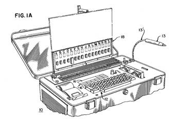
The complete PSP unit 10 is shown in FIG. 1A. A printed circuit board 18 being tested by the PSP is connected into edge connector 19 (printed circuit boards under test are referred to hereinafter as "boards under test".) It should be noted that various devices in board 18 are labeled by letters; such labeling permits the PSP to instruct the operator as to which nodes to probe during the fault isolation procedure, subsequently described in detail. Keyboard 12 permits the operator to enter data and commands into the PSP.
From Column 22, lines 40 – 49:
If the board under test does not pass the signature analysis test at each output node, the PSP then goes into an "automatic guided probe" signature analysis testing procedure wherein the display unit informs the operator, on a node by node basis, which node to probe next. The various nodes of the board under test or product under test are identified by any convenient means, such as labeling the components by letters, as shown in FIG. 1A, so that such nodes are readily recognizable by the operator.
Figure 1A, reproduced below, shows the printed circuit board to be tested (18) plugged into the tester.
The Fulks patent is for a computer-controlled digital signature analyzer used to isolate faults on digital printed circuit boards. The computer stores the signatures and other information about the board being tested and starts by performing a go/no-go test through the board’s edge connector. If the board fails, the computer directs the operator where to place a probe to read the signatures of particular circuit nodes. It then compares the signature of the nodes to the signature of the same nodes obtained from a known-good printed circuit board.
Fulks uses a separate high-speed processor (HSP 29 in Figure 2) to interface to the printed circuit board’s connector. This is succinctly explained in application 05/895,898 (now U.S. Patent 4,196,386 Method and portable apparatus for testing digital printed circuit boards issued April 1, 1980 to Phelps) incorporated by reference in Fulks. In Phelps Column 9, lines 44 – 58:
According to the present invention, a high
speed
processor (HSP), which is programmable to operate at many times the
speed of
the comparatively slow main processor is utilized to operate in
response to and
simultaneously with the main processor to sequentially route data
received in
parallel format from the main processor to predetermined ones of the
192 driver/sensor
circuits. The fast sequential outputting is accomplished by means of a
subroutine, referred to herein as an "H" file, in the form of object
code for the HSP and stored in the HSP memory. This subroutine defines
groups
of specific pins of the board under test as "destination busses" and
sequentially routes sixteen bit data words each contained in a
respective
single instruction in the test program to such "destination busses".
In Fulks, we find out that the HSP has a programmable clock. In Column 14, lines 53 – 68:
Still referring to FIG. 5, clock circuit 153 includes a number of conventional counters, registers, flip flops, and some control gating circuitry to produce high speed programmable clock signals utilized to control the operation of the HSP. The range of the cycle times of the programmable clock signals is from 150 nanoseconds to approximately 12.5 microseconds, in 50 nanosecond increments. Clock circuit 153 includes a register which is loaded from main bus 27 to determine the programmable cycle time of the HSP. The cycle time of the HSP controls the rate at which PSP 10 switches from one input/output pin to another during the testing of the board under test. Clock circuit 153 may be readily implemented utilizing Texas Instruments 74LS175 latches, 74S74 flip flops, and 74S161 counters as the main components thereof.
The central part of Fulks’ invention uses signature analysis. One of the shortcomings of signature analysis is that feedback loops must be broken. From Column 25, lines 16 – 32:
The signature analysis techniques described above "break down" if there is a feedback loop in the digital logic circuitry of the board under test. This is because an error in the response at any node in a digital feedback loop ordinarily propagates very quickly around the loop to produce faulty responses at every node in the loop, making ineffective the simple procedure of tracing along the topology pattern of a device under test until a device is found with a faulty output and all good input. As previously mentioned, all signature analysis techniques have been unsuccessful in isolating faults at nodes which occur within loops and digital circuits. Until the present invention, only expensive "factory testers" which store the entire data stream at every node, and which therefore require very large memory storage capability, have been able to isolate faults within feedback loops in digital circuits.
Fulks solves this problem by storing a smaller data stream. From Column 25, lines 33 – 43:
According to the present invention, a new procedure has been discovered which isolates faults within loops in digital circuits by determining and storing the initial state of each node in the loop and determining and storing the time at which each node in the loop initially failed. The inventive procedure has been found to compare such stored information for boards under test (with digital feedback loops therein) with data from known good boards of the same type to isolate (with a very surprisingly high degree of success) the defective components of the board under test.
Because signature analysis is at the heart of Fulks’ invention it is necessary to discuss what signature analysis is.
Signature analysis was developed several decades ago to troubleshoot printed circuit boards containing clocked logic.
Before that, the primary instrument used to troubleshoot printed circuit boards was the oscilloscope. The oscilloscope probe was connected to the various nodes and the user determined whether the signal was correct. For SSI logic this was done by first looking at the inputs and then looking at the output(s). This required knowledge of the SSI part. For larger circuits this required knowledge of how the circuit was supposed to work. The job was made somewhat easier by the development of triggered oscilloscopes with two or more channels and an adjustable delayed sweep.
Troubleshooting a logic board with an oscilloscope was frequently a painstaking, time-consuming process.
The alternative was known as shot-gunning, where integrated circuits suspected of being bad were replaced, sometimes on an educated guess, sometimes at random.
Logic Analyzers were available, which allowed a large number of digitals signals to be captured and displayed.
From Wikipedia (http://en.wikipedia.org/wiki/Logic_analyzer):
A logic analyzer displays signals in a digital circuit that are too fast to be observed by a human being and presents it to a user so that the user can more easily check correct operation of the digital system. Logic analyzers are typically used for capturing data in systems that have too many channels to be examined with an oscilloscope. Software running on the logic analyzer can convert the captured data into timing diagrams, protocol decodes, state machine traces, assembly language, or correlate assembly with source-level software.
Here is a picture of an HP 1630A Logic Analyzer.
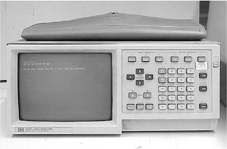
The 1630A Logic Analyzer combines four logic analysis functions in one benchtop instrument providing the versatility required in up to 35 bits and timing up to 8 bits. Features timing analysis at 100 MHz to check hardware and status signals; state analysis at 25 MHz to trace program and software flow; performance analysis to optimize code; interactive state/timing analysis to integrate circuits and code. The 1630A can become your single most important tool for logic design, development, and testing. The 1630A has 35 input lines, of which 8 lines may be used for timing analysis. Standard, built-in HP-IB and HP-IL interfaces.
The signals could be displayed as digital waveforms, as binary, or as hexadecimal. The analyzer could perform a large number of functions too numerous to list.
Using a Logic Analyzer required considerable experience. Logic Analyzers were also expensive, which made them rare, especially in the field, which made Signature Analysis more attractive..
An early patent for a Logic Analyzer is U.S. Patent 4,040,025 Logic state analyzer issued August 2, 1977 to Morrill, Jr., et al. (Assignee is The Hewlett Packard Company).
Signature Analysis was developed to allow trouble shooting to be done in the field with an inexpensive instrument.
An early patent for Signature Analysis is U.S. Patent 3,976,864 Apparatus and method for testing digital circuits issued August 24, 1976 to Gordon, et al. . (Assignee is The Hewlett Packard Company).
From the Abstract:
A device is disclosed which
converts a digital signal or bit stream into a digital signature repesentative
of the digital signal by means of a feedback shift register. The apparatus may
be used to identify and characterize digital signals at various test points in
an apparatus for testing purposes. Signatures for digital signals from properly
operating circuits can be recorded in a variety of fashions for later comparison
with signatures of digital signals from circuits under test. The comparison of
the signatures enables a person using the apparatus to determine whether the
circuit under test is operating properly and, if it is not, to locate the fault
in many instances. The apparatus may also be used to examine digital signals to
enable identification of transient errors.
In Signature Analysis the data stream from a circuit node is
clocked into a Linear-Feedback Shift Register (LFR) during a specified time
period selected by a control program. After the time period is over, the
contents of the LFR are read out and usually displayed as four non-standard
hexadecimal characters called the Signature. This signature is compared to the
signature produced by known-good hardware. The Signature Analyzer uses only four
signals: Clock, Start, Stop, and Data (from the node to be tested).
By using a LFSR, discrepancies in the data stream have a
high probability of being detected regardless of when they occur or how many
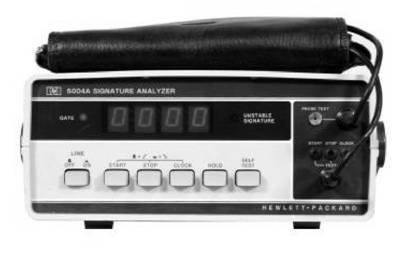
occur. See Appendix A, the Hewlett-Packard Journal for May 1977 for a detailed description of Signature
Analysis and the HP 5004A, which is pictured below.
HP5004A
There are a number of limitations of Signature Analysis which are the tradeoffs for the simplicity of the method which makes it easy to use.
1. In its pure form, feedback loops must be broken. (Fulks adds memory to record the data streams which adds to the cost and complexity of the instrument, both of which are contrary to the spirit of Signature Analysis.)
Breaking a feedback loop generally requires adding a gate to a circuit which usually increases the cost directly or indirectly because of the traces which must be added to the printed circuit board. Adding a gate also increases the propagation time of the circuit, which can reduce the system’s performance.
2. Signature Analysis is only useful for testing circuits that produce a data stream, which makes it useless for testing RAM. RAM must be tested by using a variety of data patterns. As taught in the application by the present Applicant, this is done algorithmically by following a number of steps. See Table 1(a) through Table 1(k) in the present application.
Note that although Signature Analysis can be used to test ROM in a CPU-controlled system it is more efficient for the CPU to read the Read-Only Memory locations and perform a Cyclic-Redundancy Check (CRC). This produces a checksum which can be compared to the checksum of the file data used to program the ROM. It is faster than placing a probe on each data line and it doesn’t require known-good hardware.
One of the products that used Signature Analysis was the coin-operated video game Battlezone by Atari, Inc. produced in 1980.
See Appendix B for background on the game, the Signature Analysis instructions on the schematics, and sections of the schematics showing some of the signatures.
Battlezone was one of the few games produced by Atari that used Signature Analysis. It wasn’t worth the cost. Future games used more-robust hardware design and more-comprehensive Built-In Self-Test and Diagnostic software.
It should be noted that the present Applicant, Jed Margolin, worked for Atari, Inc. and Atari Games Corporation (one of Atari Inc.’s successor companies) from 1979 – 1992.
Margolin was the Hardware Engineer for the Battlezone project. This makes Margolin a Person Having Greater-than-Ordinary Skill in this Art.
It should also be noted that Margolin is the inventor listed on U.S. Patent 4,195,293 Random dot generator for raster scan video displays issued March 25, 1980. The heart of the invention is a Linear-Feedback Shift Register. This makes Margolin a Person Having Greater-than-Ordinary Skill in this Art, too.
2. U.S. Patent 7,155,637 Method and apparatus for testing embedded memory on devices with multiple processor cores issued December 26, 2006 to Jarboe, Jr. et al. (“Jarboe”).
From the Abstract:
The disclosed method and
apparatus enables the testing of multiple embedded memory arrays associated with
multiple processor cores on a single computer chip. According to one aspect, the
disclosed method and apparatus identifies certain rows and columns within each
of the embedded memory arrays that need to be disabled and also identifies
certain redundant rows and columns in the embedded memory array to be activated.
According to another aspect, the disclosed method and apparatus generates a map
indicating where each of the memory failures occurs in each embedded memory
array. If the testing process determines that the embedded memory array cannot
be repaired, then a signal is provided directly to an external testing device
indicating that the embedded memory array is non-repairable. Similarly, if the
testing process determines that the failures in the embedded memory array can be
repaired, then a signal is provided directly to an external testing apparatus
indicating that the embedded memory array is repairable. Lastly, if no failures
are found in an embedded memory array, then a signal is provided to an external
testing apparatus indicating that the embedded memory array contains no
failures.
Here is Jarboe Figure 1:
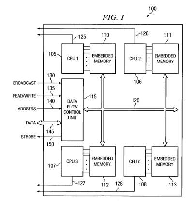
It shows a number of CPUs (processor
cores), each with its own memory. The Host uses Data Flow Control Unit 115 to
communicate with the memories. Data Flow Control Unit 115 is more than just a
multiplexor, it allows the host to write to all the memories simultaneously.
From Column 2,
lines 44 – 50:
Another aspect of the disclosed method and apparatus is a data flow control unit that controls the flow of input and output data to each of the embedded memory arrays. This device broadcasts the test program to each of the embedded memory arrays at the same time thereby enabling the simultaneous testing of multiple embedded memory arrays.
As noted, each processor has its own memory. CPU 1 (105) can access only Embedded Memory 110. CPU 2 (106) can access only Embedded Memory 111. CPU 3 (107) can access only Embedded Memory 112. Additional CPUs such as CPU n (108) can access only the Embedded Memory (113) that is associated with it.
Although Jarboe consistently refers to the Embedded Memory only as memory it is apparent that the memory is a RAM.
- The Background of the invention (Column 1, lines 36 – 42) refers to SRAMs:
As is known in the art, a memory cache often accompanies each processor on a chip. This memory cache enables the processor to operate at maximum efficiency by reducing the time required to retrieve data from memory locations outside of the chip. The memory cache associated with a processor is commonly an array of Static Random Access Memory ("SRAM") devices.
2. If the Embedded Memory were ROM the Data Flow Control Unit would not be writing to it and the only test needed would be to verify its contents.
As noted above, from Column 2, lines 44 – 50, the test program for each Embedded Memory is loaded into the Embedded Memory.
There is a problem using a processor to test its own memory when it has only that one memory.
While it is easy to detect errors caused by memory array nodes that are permanently stuck (“hard” errors) RAMs are also subject to errors caused by pattern sensitivity, which means that the data in one cell can be altered by the pattern of data in other cells (“soft” errors). See Appendix C: Semiconductor Memories - A Handbook of Design, Manufacture, and Application, Second Edition, by Betty Prince, © 1983, 1991 by John Wiley & Sons, Ltd., pages 700 – 708. Note that Ms. Prince is associated with Texas Instruments which is also the Assignee of the Jarboe patent.
When the memory being tested also contains the test program it is impossible to load the selected test pattern into the entire memory. Otherwise, it will overwrite the test program and the program will crash. As a result, Jarboe’s method cannot completely test the embedded memories for pattern sensitivity.
Moving the test program to another part of memory while its original location is being tested does not solve the problem. The result is still that the selected memory pattern cannot be written into the entire memory.
This also applies to memory locations used for storing variables as well as the program stack. This last problem can be handled if the processor has a sufficient number of registers to allow them to be used for storing variables and if the code is written to not require a program stack (i.e. no subroutines).
An example of where this was done is the Hard Drivin’ coin-operated game by Atari Games Corporation, produced in 1988. (See Appendix D)
The Main Processor is a Motorola 68010 with separate Program ROM and Program RAM. After a Power-On Reset (or a Hard Reset) the 68010 starts executing the program out of Program ROM. The first thing it does is look at the Self-Test Switch. If the Self-Test switch is not closed the 68010 starts the game. If the switch is closed the 68010 first calculates the Program ROM checksums and warns the test technician if they are incorrect. The next step is to perform the Program RAM memory test using a variety of memory test patterns. This is done without the program using the memory it is testing for its own housekeeping. The 68010 contains 16 registers. The memory test program uses some of them for storing variables. In order to not use all in-line code for the test program, some of the registers are used as Return Addresses for pseudo-subroutines. When it is desired to call a pseudo-subroutine the return address is written to a register. Then the program jumps to the beginning of the pseudo-subroutine. After the pseudo-subroutine is done it jumps to the address in the register containing the return address. The use of software macros makes it unnecessary to explicitly code every instruction.
Even so, the use of pseudo-subroutines is not transparent to the User as is the use of a Program Stack, but it allows the Program RAM to be fully tested. After the Program RAM is verified as Good, then it is available to the Program for use in storing variables and as the Program Stack.
It should be noted that the current Applicant, Margolin, was the Project Engineer and Hardware Engineer for the Hard Drivin’ project. He also specified and wrote most of the Self-Test code. This makes Margolin a Person Having Greater-than-Ordinary Skill in this Art.
3. U.S. Patent 6,035,380 Integrated Circuit issued March 7, 2000 to Shelton et al. (“Shelton”).
Shelton teaches a single chip processor for use in a smart card. Smart cards are typically used to store information representing financial transactions involving money so security is extremely important. The programs are typically stored on ROM and use sophisticated encryption methods to prevent unauthorized persons from illegally adding money to the card.
Shelton adds an additional non-volatile memory to store programs (such as card games) that can be added from third-parties.
Shelton provides an architecture that prevents this third-party software from modifying the financial software or from modifying the financial data. This is done by segmenting the memory space by using memory paging and prohibiting third-party software from changing the memory pages; the instructions that change the memory page (privileged instructions) can only be executed from ROM, not from the pages in the non-volatile memory used for third-party software. Different third-party programs are on different pages in the non-volatile memory and are therefore prevented from interfering with each other.
Data is kept in a separate non-volatile memory and is also paged so that financial data cannot be modified by third-party software.
Shelton also adds a coprocessor (cryptographic logic unit 1101) used to perform encryption tasks in order to offload it from the main (slower) processor.
This is
Shelton’s description of his invention. From the Abstract:
A single chip processor for use in a smart card has a plurality of instruction memory areas and a processor. Different instructions sets are selectively executable in response to a signal defining a memory area from which instructions are supplied. Preferably instruction and data memory areas are addressable as pages, wherein a page address cannot be directly accessed by a subset of instructions. The processor may include a central processing unit and a cryptographic logic unit which operate at different times and share common instruction memory and sequencing logic. Instructions are supplied to said cryptographic logic unit at an integer multiple of the rate at which they are supplied to said central processing unit.
Memory
Architecture
From Column 8,
lines 13 – 17:
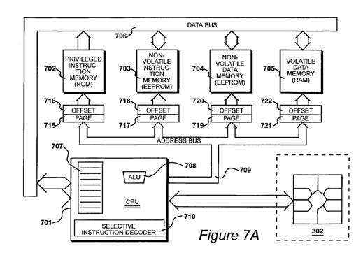
An improved memory arrangement for a smart card chip is shown in FIG. 7a. Instructions may be supplied from a privileged instruction memory 702, which is a read only memory area, or from a non-volatile instruction memory 703, which is an electrically erasable read only memory.
But only instructions coming from the ROM are allowed to change the memory page.
From Column 8, lines 30 – 46 (emphasis added):
The privileged instruction memory 702 is a read only memory area, whose contents are defined before the card is manufactured and distributed. The non-volatile instruction memory 703 may have its contents changed after the card has been distributed. For example, instructions may be updated during an interactive session with the terminal 101 shown in FIG. 1, with new instructions supplied from the large computer 107 at a remote site. The central processing unit 701, shown in FIG. 7a, includes a selective instruction decoder 710. The central processing unit has a number of possible instructions, which are referred to as an instruction set. The selective instruction decoder 710 only allows the full set of instructions to be executed from the privileged instruction memory 702. Certain instructions, particularly those which modify or read any of the page registers 715, 717, 719 or 721, are prevented from being used when they are supplied from the non-volatile instruction memory 703.
Note that new software for the financial program may be added to the non-volatile memory but will not be able to execute privileged instructions.
From Column 8, line 59 – column 9 line 13:
A representation of instructions
stored in the two instruction memory areas 702 and 703 shown in FIG. 7a, is
shown in FIG. 8. Operating system instructions 801 and serial communications
instructions 802 are stored in read only memory in the privileged instruction
memory 702. Only these instructions have full access to the instruction set, and
hence the ability to change the contents of any of the page registers 715, 717,
719 and 721. Third party applications 803 and 804, which may have been received
through a transfer at the terminal 101, are unable to access the full
instruction set, because they are stored in the non-volatile memory 703.
By preventing a third party
application from changing a page register, or jump to an instruction in another
memory area, privileged instructions may control the type of operations
performed by third party applications. For example: if third party application
803 is stored in a portion or page of non-volatile instruction memory 703
indexed by a particular page register value, it cannot directly read or jump to
an instruction in third party application 804, which is stored in a different
page of non-volatile instruction memory 703. Furthermore, page registers 719 and
721 shown in FIG. 7a cannot be directly modified by a third party
application.
Memory paging is done using the standard method used for paging memory. From Column 8, lines 18 – 22 (Referring to Figure 7a):
A page register 715 defines the most significant eight bits of the address supplied to the privileged instruction memory 702, and an offset register defines the least significant eight bits of the address supplied to the privileged instruction memory 702.
The privileged instruction memory 702 (ROM) is organized as 512 x 128 bits. Multiplexors 1202, 1203, and 1204 allow the 128-bit very-long words to be selected as 32-bit long words, 16-bit words, or 8-bit bytes. This is shown in Figure 12 which is reproduced below.
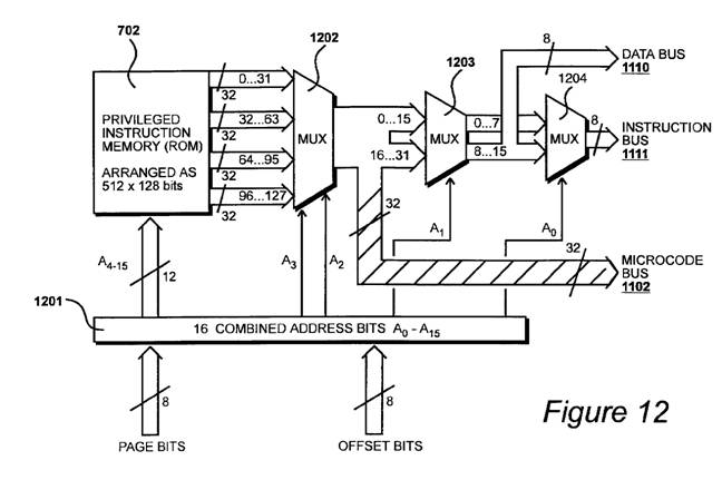
From Column 12, lines 52 – 65:
The data from each location in the privileged instruction memory is considered as comprising four lots of thirty-two bit data words, thus forming a type of cache, which are fed to a four way multiplexer 1202. One of these four words is then selected as the output of the multiplexer 1202, according to the two address lines A3 and A2 which are supplied to it. In this way, a thirty-two bit data word may be selected with an access time of fifty nanoseconds, provided the thirty two bit word was already available within the one hundred and twenty-eight bit memory array output. If this is not the case, memory control logic circuits automatically insert a wait state into the instruction fetch cycle, such that a different one hundred and twenty-eight bit word may be fetched, which contains the desired thirty-two bit word.
As shown in Figure 12, address bus 1201 is 16 bits (A0 – A15). The most significant 12 bits (A4 – A15) are used to address the ROM. This allows for 4096 very-long-words of 128 bits. (Because the ROM contains only 512 very-long-words there is room for growth.)
MUX 1202 uses address bits A2 and A3 to select among four 32-bit long words out of the 128 data bits coming from ROM 702. (32 * 4 = 128).
After MUX 1202 the 32-bit long words can be used in different ways.
1). The 32-bit long words from MUX 1202 are divided into bytes and all bytes are sent to Instruction Bus 1111.
MUX 1203 uses address bit A1 to further select between two 16-bit words from the 32-bit long word selected by MUX 1202.
All 16 bits from MUX 1203 go to MUX 1204 which uses address A0 to select between bytes containing bits (0..7) or (8..15). The byte selected by MUX 1204 goes to Instruction Bus 1111.
2). The 32-bit long words from MUX 1202 are divided into bytes. All bytes are sent to Instruction Bus 1111 but, in addition, the high byte (bits 8..15) is also sent to Data Bus 1110.
MUX 1203 uses address bit A1 to further select between two 16-bit words from the 32-bit long word selected by MUX 1202.
All 16 bits from MUX 1203 go to MUX 1204 which uses address A0 to select between bytes containing bits (0..7) or (8..15). The byte selected by MUX 1204 goes to Instruction Bus 1111.
In addition, the high byte (bits 8..15) is also sent to Data Bus 1110.
3). The 32-bit long words from MUX 1202 are sent to Microcode Bus 1102 which goes to CLU 1101 (the cryptographic logic unit).
Communications
Shelton’s smart card communicates with the outside world through communications terminals 302, which is a connector with contact pads:
From Column 5, lines 39 – 54:
The card 201 includes
communication terminals 302 allowing communication with external devices. In
particular, these terminals include a terminal for receiving a two point seven
to five point five volt power supply, a ground connection, a clock and a reset
connection. These communication terminals 302 consists of flat, gold-plated
areas of metal, which are fabricated in accordance with an international
standard for smart cards. Thus cards may be interchangeable and facilitate data
transfer in accordance with established protocols.
The communication terminals 302 are electrically and bonded
on the reverse side single silicon chip which is embedded within the smart card
substrate. Only the communication terminals 302 are actually visible on the
surface of the smart card, with the rest of the surface typically used for the
cardholder's identity, and a company logo.
And from Column 7, lines 15 – 18:
The operating system also communicates with instructions for serial communications 504, which provide the ability to transfer information to and from the outside world via the smart card terminals 302.
See Figure 3 below:
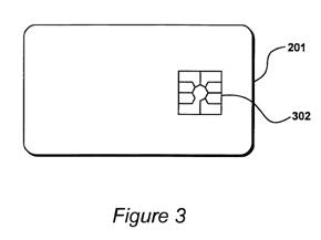
Figure 7A shows that this communications with the outside world goes through central processing unit 701.
The question may arise as to who (or what) Shelton considers a User and what he considers a User’s System.
Shelton’s User is the person who uses the smart card and the User’s System is the equipment that it is connected to through communications terminals 302 (the communications connector).
Shelton shows two types of equipment that the smart card may be connected to.
1). The smart card may be connected to a smart card terminal which is attached to a mainframe computer. From Column 3, lines 61 – 62:
Figure 1 shows a smart card terminal, a communications link, and a mainframe computer.
(In this case the communications link is between the smart card terminal and the mainframe computer.)
Figure 1 is reproduced below.
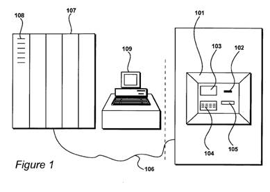
From Column 4, line 51 – Column 5, line 13 (emphasis added):
A terminal for allowing smart
card transactions is shown in FIG. 1. The terminal 101 includes a slot 102 for
receiving a smart card, a visual display unit 103 for providing the smart card user with options
and instructions for use. The user
of the smart card responds to displayed options and instructions by
pressing buttons 104, which are arranged to enable the user to provide numerical
and functional input data. A cash slot 105 is provided in the event that the user should wish to
translate money represented by data stored on the smart card into conventional
cash.
The smart card terminal
101 communicates with a large computer 107 via a communications link 106. The
computer 107 includes a large amount of data storage capacity in the form of
arrays of hard disk drives 108. A computer terminal 109 enables an operator of
the computer 107 to control access provided to smart card users via the smart card terminal 101.
For example, if a smart card is stolen, a computer operator may instruct the
computer 107 not to authorise any subsequent transfer of money to the card from
the owner's account.
Column 5, lines 4 – 13 (emphasis added):
Smart cards may be used to exchange money tokens using appropriate equipment, such as that shown in FIG. 1. Alternatively, a smaller terminal may be located alongside a supermarket checkout counter, so that a smart card may be used instead of cash. Thus, when paying for goods, the amount of money stored on the smart card is reduced. The terminal shown in FIG. 1 may be used to transfer money from the user's account, into the smart card. In this way, the same smart card may be discharged and recharged with amounts of cash, at the user's convenience.
2). The smart card may also be used with equipment that allows funds to be transferred between cards.
From Column 5, lines 14 – 26 (emphasis added):
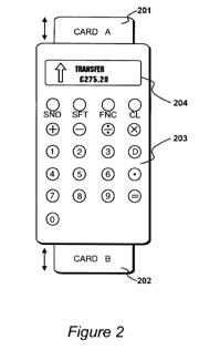
<!--[if !vml]--><!--[endif]-->Money may be exchanged directly from one smart card to another using the portable exchange device shown in FIG. 2. The portable hand held exchange device is arranged to receive a first smart card 201 and a second smart card 202. The device includes a keyboard 203 and a display device 204, providing a user interface to allow smart card users to insert their cards into the device and to specify an amount of financial token data to be exchanged between the smart cards, along with an indication of the direction of exchange. In addition, the device may also be used by the respective parties to the transaction for them to enter their personal identification numbers, as may be required in order to authorise a transaction between cards 201 and 202.
Figure 2 is reproduced to the right.
Section 2 - Examiner’s Rejections
Claim
Rejections - 35 USC § 112
Rejection 1. Claims 1-16 were rejected under 35 U.S.C. 112, second paragraph, as being indefinite for failing to particularly point out and distinctly claim the subject matter which applicant regards as the invention.
Specifically, as per claims 1, 6 and 11, lines 2 - 4, the Examiner requested interconnection and/or interrelation between the following elements and an explanation of what they are for:
a) a memory array;
b) a processor; and
c) a processor RAM memory.
As per claim 14, lines 2-4, the Examiner requested interconnection and/or interrelation between the following steps and an explanation of what they are for:
a) providing a memory array;
b) providing a
processor; and
c) providing a processor RAM
memory.
Applicant has
amended claims 1, 6, 11, and 14 as requested. Dependent claims 4, 7, 9, 12, and
13 have been canceled. Dependent Claims 2, 3, 5, 8, 10, 15, and 16 have been
amended and should be
allowable as amended.
Claim
Rejections - 35 USC § 102
Rejection 3. Claims 1-2, 6-7, 11-12 and 14-15 were rejected under 35 U.S.C. 102(b) as being anticipated by Shelton et al (6,035,380).
As per claim 1, Shelton et al disclose a single chip
integrated circuit, comprising:
(a)
a memory array (102);
(b)
a processor (701);
(c)
a processor RAM memory (705);
(d) a multiplexor (1202);
whereas said multiplexor controls and arbitrates access
between said memory array, said processor, said processor RAM memory, and
a user's system. (See Figs. 11 and 12, col. 11, lines 22-45 and col. 12, lines
10-65).
Applicant’s Response:
1. Shelton’s element 102 is not a memory array. It is a slot for receiving a smart card.
From Column 4, lines 51 – 54
(emphasis added):
A terminal for allowing smart card transactions is shown in FIG. 1. The terminal 101 includes a slot 102 for receiving a smart card, a visual display unit 103 for providing the smart card user with options and instructions for use. The user of the smart card responds to displayed options and instructions by pressing buttons 104, which are arranged to enable the user to provide numerical and functional input data. A cash slot 105 is provided in the event that the user should wish to translate money represented by data stored on the smart card into conventional cash.
Presumably, the Examiner meant to refer to Privileged Instruction Memory (ROM) 702. If this is not the case, Applicant requests clarification.
2. Shelton’s Privileged Instruction Memory (ROM) 702 is not a RAM (Read-Write Memory) as is Applicant’s memory array.
From Applicant’s specification:
[0031] Referring to Figure 1, Memory Array 106 may take several
forms. It may be a conventional read/write memory comprising row and address
decoders, a memory cell array, and sense amplifiers. The memory cell array may
be dynamic or static.
3. Shelton’s Multiplexor 1202 is part of a chain of multiplexors (Multiplexors 1202, 1203, and 1204) which allow the 128-bit very-long words produced by Privileged Instruction Memory (ROM) 702 to be selected as 32-bit long words, 16-bit words, or 8-bit bytes. This is shown in Figure 12.
The privileged instruction memory 702 (ROM) is organized as 512 x 128 bits.
From Column 12, lines 52 – 65:
The data from each location in the privileged instruction memory is considered as comprising four lots of thirty-two bit data words, thus forming a type of cache, which are fed to a four way multiplexer 1202. One of these four words is then selected as the output of the multiplexer 1202, according to the two address lines A3 and A2 which are supplied to it. In this way, a thirty-two bit data word may be selected with an access time of fifty nanoseconds, provided the thirty two bit word was already available within the one hundred and twenty-eight bit memory array output. If this is not the case, memory control logic circuits automatically insert a wait state into the instruction fetch cycle, such that a different one hundred and twenty-eight bit word may be fetched, which contains the desired thirty-two bit word.
As shown in Figure 12, address bus 1201 is 16 bits (A0 – A15). The most significant 12 bits (A4 – A15) are used to address the ROM. This allows for 4096 very-long-words of 128 bits. (Because the ROM contains only 512 very-long-words there is room for growth.)
MUX 1202 uses address bits A2 and A3 to select among four 32-bit long words out of the 128 data bits coming from ROM 702. (32 * 4 = 128).
After MUX 1202 the 32-bit long words can be used in different ways.
1). The 32-bit long words from MUX 1202 are divided into bytes and all bytes are sent to Instruction Bus 1111.
MUX 1203 uses address bit A1 to further select between two 16-bit words from the 32-bit long word selected by MUX 1202.
All 16 bits from MUX 1203 go to MUX 1204 which uses address A0 to select between bytes containing bits (0..7) or (8..15). The byte selected by MUX 1204 goes to Instruction Bus 1111.
2). The 32-bit long words from MUX 1202 are divided into bytes. All bytes are sent to Instruction Bus 1111 but, in addition, the high byte (bits 8..15) is also sent to Data Bus 1110.
MUX 1203 uses address bit A1 to further select between two 16-bit words from the 32-bit long word selected by MUX 1202.
All 16 bits from MUX 1203 go to MUX 1204 which uses address A0 to select between bytes containing bits (0..7) or (8..15). The byte selected by MUX 1204 goes to Instruction Bus 1111.
In addition, the high byte (bits 8..15) is also sent to Data Bus 1110.
3). The 32-bit long words from MUX 1202 are sent to Microcode Bus 1102 which goes to CLU 1101 (the cryptographic logic unit).
As has been explained, Shelton’s Multiplexor 1202 is used only to select among four 32-bit long words out of the 128 data bits coming from Privileged Instruction Memory (ROM) 702. Its outputs go only to Multiplexor 1203 and Microcode Bus 1102.
Multiplexor
1202 does not control
and arbitrate access between Privileged Instruction Memory (ROM) 702, CPU 701,
Volatile Data Memory 705, and Shelton’s User’s System.
Indeed, even
the chain of Multiplexors 1202, 1203, and 1202 do not control and arbitrate access
between Privileged Instruction Memory (ROM) 702, CPU 701, Volatile Data Memory
705, and Shelton’s User’s System.
Neither Figure 11 nor Figure 12 show Shelton’s User’s System.
Shelton’s User is the person who uses the smart card and the User’s System is the equipment that it is connected to through communications terminals 302 (the communications connector).
Shelton shows two types of equipment that the smart card may be connected to.
1). The smart card may be connected to a smart card terminal which is attached to a mainframe computer. From Column 3, lines 61 – 62:
Figure 1 shows a smart card terminal, a communications link, and a mainframe computer.
(In this case the communications link is between the smart card terminal and the mainframe computer.)
See Figure 1.
From Column 4, line 51 – Column 5, line 13 (emphasis added):
A terminal for allowing smart
card transactions is shown in FIG. 1. The terminal 101 includes a slot 102 for
receiving a smart card, a visual display unit 103 for providing the smart card user with options
and instructions for use. The user
of the smart card responds to displayed options and instructions by
pressing buttons 104, which are arranged to enable the user to provide numerical
and functional input data. A cash slot 105 is provided in the event that the user should wish to
translate money represented by data stored on the smart card into conventional
cash.
The smart card terminal
101 communicates with a large computer 107 via a communications link 106. The
computer 107 includes a large amount of data storage capacity in the form of
arrays of hard disk drives 108. A computer terminal 109 enables an operator of
the computer 107 to control access provided to smart card users via the smart card terminal 101.
For example, if a smart card is stolen, a computer operator may instruct the
computer 107 not to authorise any subsequent transfer of money to the card from
the owner's account.
Column 5, lines 4 – 13 (emphasis added):
Smart cards may be used to exchange money tokens using appropriate equipment, such as that shown in FIG. 1. Alternatively, a smaller terminal may be located alongside a supermarket checkout counter, so that a smart card may be used instead of cash. Thus, when paying for goods, the amount of money stored on the smart card is reduced. The terminal shown in FIG. 1 may be used to transfer money from the user's account, into the smart card. In this way, the same smart card may be discharged and recharged with amounts of cash, at the user's convenience.
2). The smart card may also be used with equipment that allows funds to be transferred between cards.
From Column 5, lines 14 – 26 (emphasis added):
Money may be exchanged directly from one smart card to another using the portable exchange device shown in FIG. 2. The portable hand held exchange device is arranged to receive a first smart card 201 and a second smart card 202. The device includes a keyboard 203 and a display device 204, providing a user interface to allow smart card users to insert their cards into the device and to specify an amount of financial token data to be exchanged between the smart cards, along with an indication of the direction of exchange. In addition, the device may also be used by the respective parties to the transaction for them to enter their personal identification numbers, as may be required in order to authorise a transaction between cards 201 and 202.
See Figure 2.
Shelton’s smart card communicates with the outside world through communications terminals 302, which is a connector with contact pads:
From Column 5, lines 39 – 54:
The card 201 includes
communication terminals 302 allowing communication with external devices. In
particular, these terminals include a terminal for receiving a two point seven
to five point five volt power supply, a ground connection, a clock and a reset
connection. These communication terminals 302 consists of flat, gold-plated
areas of metal, which are fabricated in accordance with an international
standard for smart cards. Thus cards may be interchangeable and facilitate data
transfer in accordance with established protocols.
The communication terminals 302 are electrically and bonded
on the reverse side single silicon chip which is embedded within the smart card
substrate. Only the communication terminals 302 are actually visible on the
surface of the smart card, with the rest of the surface typically used for the
cardholder's identity, and a company logo.
And from Column 7, lines 15 – 18:
The operating system also communicates with instructions for serial communications 504, which provide the ability to transfer information to and from the outside world via the smart card terminals 302.
See Figure 3.
Figure 7A shows that this communications with the outside world goes through central processing unit 701.
Thus,
Multiplexor 1202 does not control and arbitrate access between Privileged Instruction
Memory (ROM) 702, CPU 701, Volatile Data Memory 705, and Shelton’s User’s
System.
In addition, Multiplexor 1202 is only a data selector. It does not arbitrate access between anything.
From Applicant’s paragraph 0038:
[0038] Multiplexor MUX 101 controls and arbitrates access between
the internal programmable processor, Memory Array 106, and the User's system. It
allows TCPU 103 to access Memory Array 106. It also allows Memory Array 106 to
be accessed by external buses such as when the invention is used as main memory
in a User's system. In addition, through the use of the RS input on MUX 101, MUX
101 allows the User's system to control TCPU 103, access TCPU RAM Memory 104 in
order to load the program to be run by TCPU 103, and access Non-Volatile Memory
105. The BUSY output on MUX 101 tells the User's system that Memory Array 106 is
being used by TCPU 103 and to wait. The TCPU Interface contains a similar signal
to tell TCPU 103 that Memory Array 106 is being used by the User's system and to
wait. The preferred memory arbitration
scheme is to give the User's system priority to Memory Array 106. If TCPU 103 is
accessing Memory Array 106 at the beginning of a User system access, the User
system waits until the next memory cycle at which point TCPU 103 is stalled and
the User system gets access to Memory Array 106. The CLOCK input to MUX 101 is
used by TCPU 103 when the invention is used by a User's system in order to avoid
the potential for conflicts caused by metastable instability of an arbitration
logic circuit that would exist if TCPU 103 used a clock having a frequency not
synchronized to the clock used by the User's system. During Wafer testing, the
CLOCK input to MUX 101 may be used as a reference by Programmable Clock
102. In Figure 1, MUX 101 provides
external access to Memory Array 106 through a non-multiplexed address bus.
Shelton’s Multiplexor 1202 provides no such limitation. Applicant’s amended claim 1 traverses Shelton.
The Examiner has rejected
dependent claim 2, Shelton et al further comprising a
non-volatile memory (704). Applicant has traversed amended independent claim
1 over Shelton making claim 2 allowable as amended.
The Examiner
has rejected independent claims 6, 11 and 14, these
claims are rejected under similar rationale as set forth in claim 1. Applicant traverses amended
independent claims 6, 11, and 14 over Shelton under the same rationale as set
forth in traversing Shelton over amended claim 1.
The Examiner
has rejected dependent claims 7, 12 and 15, these claims
are rejected under similar rationale as set forth in claim 2. Applicant has
canceled dependent claims 7 and 12. Applicant has traversed the amended independent claim 14
over Shelton making dependent claim 15 allowable as amended.
Rejection 5. Claims 3, 8, 13 and 16 were rejected under 35 U.S.C. 103(a)
as being unpatentable over Shelton et al (6,035,380) in view of Fulks et
al (4,194,113).
As per claim 3, the teaching of Shelton et al have been
discussed above. Shelton et al further disclose a clock circuit (Fig. 14).
They do not disclose that the clock circuit is a
programmable clock. However, Fulks et al disclose a programmable clock (153). (See Fig. 5,
col. 14, lines 53-68). Therefore, it would have been obvious to a person of ordinary skill
in the art, at the time the invention was made, to incorporate the programmable
clock as taught by Fulks et al into the clock circuit of Shelton et al so
that it can produce a high speed programmable clock signals utilized to
control the operation of a high speed processor (HSP). (See col. 14, lines
53-68).
As per claims 8, 13 and 16, these claims are rejected under
similar rationale as set forth in claim 3.
Applicant’s Response:
1. Shelton has been traversed above in Rejection 3 above.
2. The Fulks patent is for a computer-controlled digital signature analyzer used to isolate faults on digital printed circuit boards. The computer stores the signatures and other information about the board being tested and starts by performing a go/no-go test through the board’s edge connector. If the board fails, the computer directs the operator where to place a probe to read the signatures of particular circuit nodes. It then compares the signature of the nodes to the signature of the same nodes obtained from a known-good printed circuit board. See Column 6, lines 3 – 6, Column 6, lines 29 – 38, Column 22, lines 40 – 49, and Figure 1A.
The central part of Fulks’ invention uses signature analysis. One of the advantages of signature analysis is that it does not require the storage of the entire data stream at every node, and which therefore require very large memory storage capability. See Column 25 lines 28 – 31.
One of the shortcomings of signature analysis is that feedback loops must be broken. See Column 25, lines 16 – 32. Fulks solves this problem by storing a smaller data stream. See Column 25, lines 33 – 43.
Fulks uses a
separate high-speed processor (HSP 29 in Figure 2) to interface to the printed
circuit board’s connector. This is succinctly explained in application
05/895,898 (now U.S. Patent 4,196,386 Method and portable apparatus for
testing digital printed circuit boards issued April 1, 1980 to Phelps) incorporated by
reference in Fulks. See Phelps Column 9, lines 44 – 58:
According to the present
invention, a high speed processor (HSP), which is programmable to operate at
many times the speed of the comparatively slow main processor is utilized to
operate in response to and simultaneously with the main processor to
sequentially route data received in parallel format from the main processor to
predetermined ones of the 192 driver/sensor circuits. The fast sequential
outputting is accomplished by means of a subroutine, referred to herein as an
"H" file, in the form of object code for the HSP and stored in the HSP memory.
This subroutine defines groups of specific pins of the board under test as
"destination busses" and sequentially routes sixteen bit data words each
contained in a respective single instruction in the test program to such
"destination busses".
In Fulks, we find out that the HSP has a programmable clock. In Column 14, lines 53 – 68:
Still referring to FIG. 5, clock circuit 153 includes a number of conventional counters, registers, flip flops, and some control gating circuitry to produce high speed programmable clock signals utilized to control the operation of the HSP. The range of the cycle times of the programmable clock signals is from 150 nanoseconds to approximately 12.5 microseconds, in 50 nanosecond increments. Clock circuit 153 includes a register which is loaded from main bus 27 to determine the programmable cycle time of the HSP. The cycle time of the HSP controls the rate at which PSP 10 switches from one input/output pin to another during the testing of the board under test. Clock circuit 153 may be readily implemented utilizing Texas Instruments 74LS175 latches, 74S74 flip flops, and 74S161 counters as the main components thereof.
Thus, Fulks’ programmable clock is used with the HSP 153 which contains drivers/sensors for interfacing with the pins on the edge connector for a printed circuit board.
Fulks’ invention could not be more different from Applicant’s invention.
1). Fulks’s invention is embodied in an instrument (and a fair-sized instrument at that; see Figure 1A) for testing printed circuit boards using signature analysis and contains a limited amount of storage for storing data streams.
2). Signature analysis compares the signatures from the board under test to the signatures obtained from a known-good board.
3). Signature analysis is not used for testing RAMs.
4). Applicant’s invention is a single chip memory with an embedded processor (TCPU 103) with its own separate memory (TCPU RAM 104) for testing the RAM (Memory Array 106), all in Applicant’s Figure 1. The memory test program performed by TCPU 103 does not use signature analysis and does not store data streams; it performs an algorithmic test of Memory Array 106. See Table 1(a) through Table 1(k). The Applicant’s invention is not a test instrument and does not test printed circuit boards.
Thus, although Fulks shows a programmable clock with HSP 153, Fulks teaches away from Applicant’s invention.
Rejection 6. Claims 4-5, and 9-10 were rejected under
35 U.S.C. 103(a) as being unpatentable over Shelton et al (6,035,380) and
further in view of Jarboe, Jr. et al (7,155,637).
As per claims 4-5, the teaching of Shelton et al have been
discussed above. They do not disclose that a program is used by the processor to
test the memory array. However, Jarboe, Jr. et al disclose that the program is
used by the processor to test the memory array (col. 5,
lines 53-63). Therefore, it would have been obvious to a person of ordinary
skill in the art, at the time the invention was made, to incorporate the program that is used by the
processor to test the memory array as taught by Jarboe, Jr. et al into
the invention of Shelton et al so that test program can be used to test memory
array to detect errors and the test program can be stored in the processor RAM
memory for relater used.
Applicant’s Response:
1. Shelton has been traversed above in Rejection 3 above.
2. Jarboe’s test program is used with memories containing redundant rows and columns that can be activated to replace defective rows and columns discovered during testing.
From the Abstract:
The disclosed method and
apparatus enables the testing of multiple embedded memory arrays associated with
multiple processor cores on a single computer chip. According to one aspect, the
disclosed method and apparatus identifies certain rows and columns within each
of the embedded memory arrays that need to be disabled and also identifies
certain redundant rows and columns in the embedded memory array to be activated.
According to another aspect, the disclosed method and apparatus generates a map
indicating where each of the memory failures occurs in each embedded memory
array. If the testing process determines that the embedded memory array cannot
be repaired, then a signal is provided directly to an external testing device
indicating that the embedded memory array is non-repairable. Similarly, if the
testing process determines that the failures in the embedded memory array can be
repaired, then a signal is provided directly to an external testing apparatus
indicating that the embedded memory array is repairable. Lastly, if no failures
are found in an embedded memory array, then a signal is provided to an external
testing apparatus indicating that the embedded memory array contains no
failures.
There is no suggestion that Fulks’ memory array contains redundant rows and columns that can be used to repair defects in the memory array.
Therefore, there would be no motivation to use Jarboe’s memory test program in Fulks.
Section 3.
For the foregoing reasons, Applicant submits that all
objections and rejections have been overcome. Applicant requests that the
rejection of pending claims 1, 2, 3, 5, 6, 8, 10, 11, 14, 15, and 16 be
withdrawn and that the application be allowed as amended.
Respectfully submitted,
/Jed Margolin/
Date: September 20, 2007
Jed Margolin
Jed Margolin
1981 Empire Rd.
Reno, NV
89521-7430
(775) 847-7845
______________________________________________________________________
Appendices:
Appendix A -
Hewlett-Packard Journal (HP Journal) May 1977, Pages 2 - 21
Appendix B -
Appendix C -
Semiconductor Memories - A Handbook of Design, Manufacture, and Application,
Second Edition, by Betty Prince, © 1983, 1991 by John Wiley & Sons, Ltd.,
pages 700 – 708.