Standalone Controller for an IDE CDROM Drive
or
The Secret Life of CDs
by Jed Margolin
Originally posted: January 2001
Update:
February 2003
This project started out because I wanted to read the digital data from a CDROM Drive and stream it to a DSP Evaluation Board containing an Analog Devices ADSP-2181 in order to build a standalone Simulated AM Radio. The purpose was to demonstrate the principles contained in a patent application that was eventually allowed and issued as U.S. Patent 5,978,488 Simulated AM Radio. (You can read the patent here .)
At some point I realized that with some changes I could use it to enter Motorola's Design 99 contest which was sponsored by Motorola (and run by Circuit Cellar Magazine) to come up with applications for Motorola's newly introduced 68HC908GP20 microcontroller.
In 1999 the cost of CD Burners was coming down and people were making their own backup copies (and compilations) of their Audio CDs. Although most consumer CD Players would play CDRs there were few, if any, that played CDRWs. I expect that, by now, most do. (A CDRW is a good way to test whether the disc you made works the way you want.)
By then, most computer CDROM Drives would play CDRWs, and since the ability to play audio CDs is part of the CDROM specification, I felt that a small standalone controller had some value.
Motorola agreed, at least to the extent that I won one of the Second Place prizes.
Once I started my own Web site I posted the article.
Since then the project has become old and creaky.
Motorola never put the 68HC908GP20 into production. Instead, they produced the 68HC908GP32. The GP32 is almost identical to the GP20 except it has more user Flash Memory and they moved one register. (The software I wrote fits in the GP32 memory space and I wasn't using the register that was moved, so the original software runs in a GP32 without modification.)
Based on comments I have received from people interested in the project I have made a few hardware and software changes.
Here are the highlights.
1. The updated project contains an on-board GP32 programmer that works with the P&E Microsystems Programming software. It also works with their Debugger software. The P&E Microcomputer Systems software is available for free from their web site. (Thank you, P&E Microcomputer Systems.)
2. In order to work with the P&E Microcomputer Systems Debugger I have rewritten the software. It is incompatible with the old software if you were using it to do development. (Of course, you don't have to change your hardware/software if you don't want to.) The original article is posted here.
Introduction
This project uses a Motorola 68HC908GP32 to control an IDE (ATAPI) CDROM Drive. It also has a 2x20 line LCD Display, six pushbutton switches, an RS-232 serial interface, and a connector for the SPI port. The original project also had a header for emulating 68HC705P6 and 68HC805P18 microcontrollers. Since I don't work with these parts anymore there was no point in keeping it, so I have taken it off.
I would characterize this project as somewhere between Intermediate and Advanced. I don't think this would be a good project for a Beginner unless you are willing to spend a great deal of time on it. (But if you do, you will learn a great deal in the process.)
If you are going to build this project
there is some documentation and software you should have, so let's do that
first.
GP32 Documentation
The 68HC908GP32 products page is at:
http://e-www.motorola.com/webapp/sps/site/prod_summary.jsp?code=68HC908GP32&nodeId=01624684498634
This contains a great deal of documentation including application notes.
Warning:
1. The page does not like Netscape 4.51 (which is my preferred browser).
2. If you want to download software listings you have to register. If you want to register, it refuses to let you in if you are using MSIE with cookies restricted to the originating server. At least, that's what I think the problem is. I ended up using Mozilla for downloading the software.
Assuming this specific link works, here is the Data Manual for the GP32:
http://e-www.motorola.com/brdata/PDFDB/docs/MC68HC908GP32.pdf
The Programming Manual for the HC08 series is at:
http://e-www.motorola.com/brdata/PDFDB/docs/CPU08RM.pdf
You may also be able to get Printed Manuals.
The actual page cannot be bookmarked, so you have to go to the 68HC908GP32
products summary page:
http://e-www.motorola.com/webapp/sps/site/prod_summary.jsp?code=68HC908GP32&nodeId=01624684498634
Find: Other Info
Select: Literature Services
This will take you to
http://merchant.hibbertco.com/mtrlext/
Select General Search on the left menu.
Do a search using Document Number: "MC68HC908PG32/D"
This will allow you to download it and/or get a printed copy.
Do a search using Document Number: CPU08RM
This will allow you to download it and/or get a printed copy.
This might be a good time to explain the differences between the GP32 and the GP20 that was used in the original project. The GP32 appears to be the same as the GP20, except for two things:
1. In the GP32, the FLASH Block Protect Register (FLBPR) is located at address $FF7E.
In the GP20, the FLBPR is located at $FF80.
The programs in the original article and this updated article do not
use the FLBPR Register so this change has no affect on the code.
2. The GP32 has 32,256 bytes of Flash Memory, located $8000 - $FDFF.
The GP20 has 19,968 bytes of memory, located in $B000 - $FDFF.
The program in the original article and this updated article fit in the larger program space without any problem.
I have programmed the code from the original article into a GP32 with no modifications to the code, and the program works just fine.
The code for this updated article works
with either a GP20 or a GP32 with no modifications.
Optrex LCD
This project uses the Optrex DMC20261 20x2 LCD display. The datasheet for it is here . I used it because when I did the project they were cheap and easy to get. That might not be true today.
The DMC20261 uses the Hitachi HD44780U Controller. There are a great many LCD displays that use this controller so they should work with the software. Obviously, if you use a smaller LCD (like a 16x2) you will have to figure out where to put the messages that were designed for the 20x2 display.
Although this project uses only the built-in character set, the HD44780U allows you to use its internal RAM to define (and use) a limited number of your own characters and symbols.
To make things easier for you, here is
the datasheet for the HD44780U.
P&E Microcomputer Systems Software
From the P&E Microcomputer Systems homepage (www.pemicro.com):
"P&E Microcomputer Systems is an industry trendsetter in hardware and software development tools for Motorola microcontrollers. P&E takes pride in its commitment to providing professional, low-cost development tools and prompt, knowledgeable customer support."
To get the software for the GP32:
Go to their home page: www.pemicro.com
Select: In-Circuit Debugger Resource Page
Then Select: 68HC08
Then Select: ICS08GPGT Software for 68HC908GP32/GT16/GT8
Single File Install (32-bit) v. 1.43A
(You will need to register at the bottom of the page before you can download it.)
Once you have downloaded it, install it by running it.
After installing it I went to the directory where I told it to live and sent shortcuts to my desktop for: prog08sz.exe (the Programmer), icd08sz.exe (the Debugger), and ics08gpgtz.exe (the Simulator). I also copied the assembler casm08z.exe to my own directory to make it easy to call from a batch file. My batch file (casm.bat) contains the single statement:
\gp32\casm08w.exe %1 S L D C
S
- generates a Motorola S19 object file
L - produces a program listing
D - produces a P&E Debug map file
C - shows cycle counts in the list file
It's called by typing: casm <filename>
You can see all the options by running casm08z with no arguments.
IDE Interface Documentation
The Compact Disc (audio) was brought out in 1982 by Philips and Sony. (For a history of the Philips effort see reference [2].) Since there was no external interface, manufacturers were free to design the system however they wanted to.
The standard for using Compact Discs for storing digital data came out in 1984 but CDROMs did not catch on right away. CDROM drives were expensive, as were the CDROM products. CDROM drive interfaces were either SCSI or proprietary to the manufacturer.
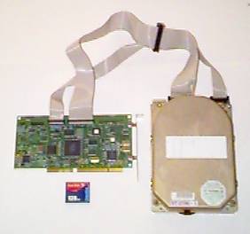
It wasn't until 1993 that a standard using the IDE interface was announced [3]. The IDE (Integrated Drive Electronics) interface was created by CDC, Western Digital, and Compaq for hard disk drives and was first used in 1986. Before that you used a separate controller card for your hard drive. My first IBM PC/Clone (1990) came with a Western Digital ST-277R 60Mbyte Hard Drive and an ISA controller card. See picture (For reference, the small square thing is a 128Mbyte Compact Flash Card.) And speaking of the ISA bus, the IDE interface started out as the ISA bus minus the signals it didn't need but it has evolved to have more capabilities and greater speed than the ISA bus.
The IDE interface is officially known as the ATA (AT Attachment) Interface. The standard for CDROM drives is called ATAPI (AT Attachment - Packet Interface).
The IDE Interface is register-based and allows for Direct Memory Access (DMA) for the transfer of data. Data can also be transferred through the registers. This is called Programmed I/O (PIO).
The IDE Interface consists of:
16 bidirectional data lines
3 address lines
2 chip selects (address block select)
lines
as well as several control lines and flag inputs.
The three address lines and two chip selects allow for two address blocks of eight registers.
One chip select is used for an address block of eight registers. The other chip select accesses only two registers; the other six are reserved for a floppy disk controller. The basic operation of the IDE interface can be found in reference [4]. By now this reference is probably difficult to find. A description of the IDE interface can be found in the ATA\ATAPI reference d1532v2r1a.pdf (1.7 Mbyte PDF), Section 8 Interface Signal Assignments and Descriptions. This reference will be discussed very shortly.
ATAPI (ATA Packet Interface)
Although both ATA and ATAPI have similar registers, some are used differently and have been given different names. See Table 1 for ATA register names and Table 2 for ATAPI register names.
One of the challenges in using the IDE bus for CDROM drives was to allow two different types of devices, each with its own software driver, to coexist on the same bus. Moreover, it had to work with software already in the field. For example, a command to reset the CDROM drive must not also reset the hard drive because the software driver for the hard drive would probably be unaware that its drive had been reset.
The solution was to use an unimplemented ATA command to reset the ATAPI device. Similarly, an ATA reset command is not recognized by an ATAPI device.
At this point you might be wondering why CDROMs needed a different interface protocol? Why not just treat it as a read-only hard disk drive?
The answer appears to be the decision to make the interface as much like SCSI as possible in order to preserve the manufacturers' investment in software and firmware.
Yes, the ATAPI standard is modeled after SCSI.
However, considering the number of CDROM Drives that have been sold and the fact that most of them use the IDE Interface, this is another case of the Tail Wagging the Dog. (The SCSI-modeled command structure is a pain-in-the-ass to implement.)
The ATAPI standard was originally called SFF-8020i . (SFF stands for Small Form Factor.) SFF-8020i provides all the information needed to control the CDROM drive. It provides commands for opening and closing the tray, reading data, and playing audio CDs. There are even commands for telling the CDROM to identify itself and its capabilities. This is the reference I used for writing the program.
At some point SFF-8020i became INF-8020i. This has since become folded into the general ATA/ATAPI specification. You can download the latest pre-release version for free from the web site of the T13 Technical Committee. From their home page:
"T13 is a Technical Committee for the InterNational Committee on Information Technology Standards (INCITS). INCITS is accredited by, and operates under rules approved by, the American National Standards Institute (ANSI)."
As of this writing in February 2003 the current version is 1532D AT Attachment - 7 with Packet Interface (ATA/ATAPI-7) d1532r1a .
It comes in two parts: Volume 1, available at: www.t13.org/docs2002/d1532v1r1a.pdf (1.7 Mbyte PDF) and Volume 2 available at: www.t13.org/docs2002/d1532v2r1a.pdf (2.3 Mbyte PDF).
Frankly, if your primary interest is in making something to talk to a CDROM Drive, having the ATAPI (ATA Packet Interface) standard part of the ATA standard means you end up wading through a great deal of material that does not apply to your application.
Therefore, I am posting the original SFF-8020i specification (785 Kbytes, PDF). Presumably, there are errors in it and it does not contain the bells and whistles supported by the latest CDROM Drives, which is why it was superseded. If you use SFF-8020i I suggest you check the commands you use against the ATA/ATAPI standard, especially if something you try to do doesn't work.
If I am asked to remove this document by
a representative of the Small Form Factor Committee, or by whatever entity
has reasonable claims to the material, naturally I will promptly comply.
Serial Port Capture Software
Because the updated project is oriented to the use of the P&E Microcomputer Systems software, and their software connects to the PC Host with an RS-232 Serial port, I have found it essential to be able to capture the data from the Serial Port in order to write the software which will be described later.
The software I used was the beta version of Comlab32 Serial Port Capture program which was available (for free) from RealTime Control at: www.rtcomm.com/comlab32.html .
From their homepage:
"Realtime Control, Inc. is an embedded systems provider, specializing in customizable high-speed serial communications hardware and software. Our product lines feature serial coprocessors capable of synchronous and asynchronous operation supporting the RS232 and RS485 standards."
In the version I have, the Print function has not been implemented.
In order to print the data I use the "Print Screen" function in
Windows 98SE and paste it into Microsoft Word.
Operating Modes
The project has three major operating modes.
Mode 1: User
Mode 1 presents the user with four options:
1.) A standalone controller for an IDE (ATAPI) CDROM Drive for playing audio CDs. The value in this is that if the CDROM Drive is able to play CDRW discs, then it will play audio CDs recorded on CDRW discs.
CDRW discs have a lower reflectance value than CDROM or CDR discs. At the time this project was done very few consumer CD Players could play them, while, by then, most CDROM Drives did support CDRW discs.
2.) Display several of the more interesting capabilities of the CDROM Drive, namely Manufacturer, Model Number, types of discs it supports (CDROM, CDR, CDRW), the size of the buffer, the drive's maximum speed, and whether it supports multisession discs.
3.) Display the GP32's Security Code ($FFF6-$FFFD).
4.) Run a test program. Currently, this program toggles a bit
(PTD0) every 1ms. This was originally done to verify the timing of the
MCU. I kept it in to allow users to easily try out their own code.
Mode 2: Development (Debugger)
In Mode 2, the unit connects to a PC Serial Port and runs my own version of the Motorola Monitor program so the unit could be used with the P&E Microcomputer Systems Debugger program. It was necessary to write my own version of the Motorola Monitor Code in order to move the Serial Port from PTA0 to PTE0, to allow the MCU to operate at full speed (32 MHz clock = 8 MHz Bus), and to operate at 19,200 Baud.
The Motorola Monitor lives in its own memory space in each GP32 and is entered through various means. Unfortunately, it uses PTA0 (Bit 0 of Port A) for Serial Communications with the Host PC. Port A is one of the two 8-bit ports and is needed for the IDE Interface and for the LCD. The Motorola Monitor also presents the user with a limited choice of clock frequencies, either 4.9152 MHz or 9.8304 MHz. Because Monitor Mode divides the clock by either 2 or 4 it means the Bus clock in Motorola Monitor Mode will be either 2.4576 MHz or 4.9152 MHz.
Since the GP32 is rated to operate at a maximum Bus Clock of 8 MHz, it would mean pissing away either 39% or 69% of the CPU processing capacity during debugging.
When using it with the P&E Microsystems Debugger, select the Serial
Port you are using, and select 19,200 Baud. The Interface is "Class
III - Direct serial to target w/MONO 8 serial port circuitry built in."
Mode 3: Programmer
Mode 3 is an in-circuit GP32 Programmer that operates with the P&E Microcomputer Systems Programmer software. For various reasons this can only be done using the Motorola Monitor. Thus, during programming, the MCU clock is changed from 32 MHz to 9.8304 MHz and the Serial port is changed from PTE0 to PTA0.
Although you can also use the P&E Microcomputer Systems Debugger with the unit in Mode 3, you will not be able to use the LCD or the IDE Interface because PTA0 is used as the Serial port. The GP32 will also run slow as noted above.
The P&E Microsystems Programmer software uses the same serial port setup as the Debugger. If you have not already set it up, select the Serial Port you are using, and select 19,200 Baud. The Interface is "Class III - Direct serial to target w/MONO 8 serial port circuitry built in."
Motorola Monitor
Since the primary purpose of this update is to support in-circuit programming and debugging with P&E Microcomputer Systems' Host PC software, a discussion of Motorola's Monitor Mode is in order. I suggest you read Section 15 Monitor ROM (MON) MC68HC908GP32 Data Manual. (The method for getting it was covered in this article in the section GP32 Documentation.)
Each GP32 contains a Monitor ROM (307 bytes) located at $FE20 - $FF62. When the GP32 is in Monitor Mode the Reset and SWI vectors are taken from addresses $FEFC - $FEFF instead of $FFFC - $FFFF (where the User's vectors live).
The Monitor Mode code has a software UART for communicating with the Host PC and implements a small number of commands:
Read
Memory
Indexed Read Memory
Write Memory
Indexed Write Memory
Read Stack Pointer
Run
Since Monitor Mode is called by its initialization code issuing an SWI instruction, the Run instruction simply performs an RTI instruction.
To cause the GP32 to execute code at a specific address the Host PC reads the Stack Pointer and writes the address of the code to be executed at the locations in the Stack containing the RTI address.
The Debugger works by using the BreakPoint Registers which generate an interrupt when the GP32's address matches the address contained in the Break Register, in which case when the Host PC instructs the Monitor to do an RTI it resumes execution from where it left off, in the code (presumably yours) that you are debugging.
Getting into Motorola's Monitor Mode is a decision made by the hardware during Power-On Reset (POR) and presents the hardware designer with several choices, most of which are unpleasant.
There are several ways to get into Monitor Mode.
1. If the part is blank, both $FFFE and $FFFF = $FF. ($FFFE and $FFFF are the Reset Vector)
If the IRQ input = logic '1' and PTA0 = '1'
the bus clock will be the external clock/4.
(According to Table 15-1 it also expects PTA7 to be '0'.)
For an external clock of 4.9152 MHz the Serial I/O will
be 9600 Baud.
If the IRQ input = '0' and PTA0 = '1' the PLL will be used
and will expect an external clock frequency of 32.768 KHz.
(According to Table 15-1 it also expects PTA7 to be '0'.)
The Serial I/O will be 9600 Baud.
If the part is not blank (either $FFFE or $FFFF is not $FF) it goes into User Mode regardless of the state of IRQ.
2. If the IRQ input = VTST (minimum is VDD+2.5V, maximum is 9.1V) it looks at PTC0, PTC1, PTC3, PTA0, and PTA7.
PTC0 PTC1 PTC3 PTA0 PTA7
Bus Clock
1 0
0 1 0
External Clock/2
1 0
1 1 0
External Clock/4
With an External Clock of 4.9152 MHz:
Bus Clock = External Clock/2
= 2.4576 MHz produces a Serial I/O Baud Rate of 9600 Baud.
With an External Clock of 9.8304 MHz:
Bus Clock = External Clock/4
= 2.4576 MHz produces a Serial I/O Baud Rate of 9600 Baud.
However, if you use an External Clock of 9.8304 MHz and use External
Clock/2 (PTC3 = '0'):
Bus Clock = External Clock/2
= 4.9152 MHz produces a Serial I/O Baud Rate of 19200 Baud.
Changing the Bus Clock does not affect the programming parameters because the P&E Microcomputer Systems Programmer software determines the speed of the GP32 and adjusts the programming parameters accordingly.
The following discussion will be easier to understand if you download the following circuits.
Circuit P1 (PDF) is the Figure 15-1 Monitor Mode circuit from the 68HC908GP32 Data Manual.
Circuit P2 (PDF) is the Figure 9-3 Monitor Mode Circuit (External Clock, with High Voltage) from the 68HC908QY/QT Data Manual.
Circuit P3 (PDF) is the Figure 1. Low-Cost Evaluation Board Schematic from Application Note AN2305 for the 68HC908QY/QT.
Circuit P4 (PDF) is a simplified version of my programmer for the GP32. It's what the GP32 in the current project sees when it is in Program Mode.
Circuit P1 shows the GP32 Monitor Mode Circuit in all its glory, with all its options and configurations. Look at all the switches.
Since all we want to do is be able to program the part we only need one configuration. That will makes things much simpler.
The configuration I chose was:
PTC0 PTC1 PTC3 PTA0 PTA7
Bus Clock
1 0
0 1 0
External Clock/2
With an External Clock of 9.8304 MHz the Bus Clock = External Clock/2 = 4.9152 MHz and produces a Serial I/O Baud Rate of 19200 Baud.
The reason I did not choose one of the modes that requires that the part be blank is that after you have programmed it the first time it is no longer blank. You would have to either remove it from the board and erase it in a separate Programmer or you would have to give your software the ability to erase itself on the board. While it is feasible to do this, it would mean that if you made a mistake while you were working on the code you might not be able to call the Erase function, so you would have to remove the GP32 from the board and erase it in a separate programmer.
Note in circuit P1 that Motorola used their own MC145407 TTL/RS-232 level translator IC. You can't really blame them for using a Motorola part. That doesn't mean we have to use it. The Maxim MAX-232 is more popular and has several second sources, so that's what we will use.
Note in Circuit P2 several items of interest.
1. Even Motorola switched over to the MAX-232.
2. VTST is derived from the V+ output of the MAX-232.
In order to translate TTL levels to RS-232 levels the MAX-232 contains two voltage pumps. One produces >+12V (V+); the other produces <-12V (V-).
The MAX-232 is able to produce a little more current at V+ and V- than it needs so using V+ for VTST is a good idea because VTST requires very little current. (The GP32 contains its own charge pump to provide the high voltage for programming the Flash Memory. VTST is only used to get it into Monitor Mode.)
I have a problem, however, with Motorola's choice of Zener diode.
Note that they used a 9.1V Zener.
Zeners come with a voltage tolerance rating, generally either 5% or 10%.
A 9.1 Volt Zener will therefore be in the range of 9.1V plus or minus 5%, which comes out to a range of 8.645V to 9.555V.
A 10% Zener will be in the range of 8.19V to 10.01V.
Therefore, assuming a normal distribution of zener values (and without any other information, that is what we must assume) regardless of whether the Zener tolerance is 5% or 10%, half of all 9.1V Zeners will produce a voltage greater than 9.1V .
According to the MC68HC908GP32/D Data Manual, Section 23.6, VTST has a maximum value of 9V . (In later parts like the 68HC908QY4 they specify 9.1V so for the purposes of discussion we will assume 9.1V.)
An 8.2V 5% Zener will have a voltage range of 7.79V to 8.61V. Since the minimum VTST for entering Monitor Mode is VDD+2.5V (again from Table 18.6) and assuming the GP32 is operated at 5.0V (giving VTST Minimum of 7.5V), an 8.2V 5% Zener is the correct part to use.
An 8.2V 10% Zener will have a voltage range of 7.38V to 9.02V, and is therefore not guaranteed to put the GP32 into Monitor Mode.
If you are building your own Programmer you can hand select the Zener if you know you have to.
In a production environment, hand selection is a huge waste of money since it is cheaper to just buy the correct part, which in this case is an 8.2V 5% Zener.
Note that this Zener is not a rarely used clamp.
The MAX-232 produces a positive voltage somewhere above 12V. The Zener is a voltage regulator that is used whenever the GP32 is being programmed.
End of Rant (about VTST).
Next, your attention is drawn to circuit P3 from Application Note AN2305 for the 68HC908QY/QT which shows the 74HC125 replaced by Resistor R3 and Diode 1N4148. I have seen this circuit in other Motorola literature where they refer to it as suitable for "low speeds". It works fine at 19200 Baud so let's use it.
I have combined all these elements in circuit P4. It's what I was going
to build before I decided to incorporate the GP32 Programmer on-board the
current project. Pot KP1, Resistor R5, and LED D4 were intended for use
in trying out simple programs on the Programmer Board. Diode D1 is to protect
the board from a reverse polarity DC voltage supply. With the exception
of these parts, circuit P4 is what the GP32 in the current project sees
when it is in Program Mode.
GP32 Security
After entering Monitor Mode by one of the above methods, the GP32 Security feature is activated. Here's how it works:
After a Power-On Reset (POR) in User Mode: All memory is accessible.
After a POR in Monitor Mode:
1. All memory is accessible so the Internal Monitor Code can check the Security Bytes ($FFF6-$FFFD, which is in the User Vector Table). The Host PC sends these bytes to the GP32 Monitor which does the comparison.
2. If the Security Code matches, it takes the last data it received (which would be from $FFFD) and writes it to $FFFF. All memory remains accessible.
3. If the Security Code does not match, it reads $FFFF, and Security Mode makes Flash Memory inaccessible.
The data written to $FFFF after a successful Security Code match may be irrelevant and it is only whether the first access to $FFFF is a write or a read that matters.
The Security Mode remains as selected until another Power-On Reset, so that a Security Code failure requires another Power-On Reset.
Here is the Monitor Code that is run at the start of Monitor Mode and does the Security Code checking:
*******************************************************************
* Monitor Initiation/Check Security Code
*==================================================================
001
ORG $FF00
002
003 START: BIH br31
; If IRQ is high, do direct clock
004
005 * Set up the PLL
006 * Monitor Mode uses a VCO clock of 9.8304
MHz, Bus frequency = 2.4576 MHz.
007
CLR PCTL
; PLL Control -> P,E
008
BSET 0,PCTL ; PCTL
= $01
009
BSET 0,PMSH ; PLL
Multiplier Select High byte
010
LDA #$2C
011
STA PMSL
; PLL Multiplier Select Low byte
012
LDA #$80
013
STA PMRS
; PLL VCO Range Select ->L
014
BSET 5,PCTL
015
BSET 7,PBWC ; PLL
Bandwidth Control
016
017 loop1: BRCLR 6,PBWC,loop1
; wait for PLL to stabilize
018
BSET 4,PCTL ; select
VCO clock
019 *----------------------------------
020 * Clock is set up, either Direct External
Clock or PLL
021 br31: AIS #-6
; reserve some stack space (why?)
022
BCLR 0,PORTA ; used in
SENDCHAR later on
023
MOV #$0FF,sflag ; security flag
024
LDHX #$0FFF6 ; first address
of security code
025
BRSET 7,PORTA,br32 ; When PA7 = 1 it will use parallel data
input
026
BCLR 7,sflag ; PA7 = 0
for serial data input
027 *----------------------------------
028 * If it is using parallel data input it will
read the security data from
029 * Port A and skip GETCHAR. It
does not signal the outside world when it is
030 * reading the port. Apparently
data must be presented to Port A by using
031 * rigorous timing.
032 br32: CBEQX #$0FE,INITOUT1
; compare XReg, no flags affected
033
LDA PORTA
; parallel data input
034
BRSET 7,sflag,br34 ; skip GETCHAR if using parallel data input
035
036
JSR GETCHAR ; Returns
with a character in ACC
037
038 br34: NOP
039
CBEQ X+,br32 ; compare
ACC to iX+, no flags affected
040 *----------------------------------
041 * something didn't match, but don't tell
anyone yet
042 br41: CBEQX #$0FE,INITOUT2
; compare XReg, no flags affected
043
LDA PORTA
; parallel data input
044
BRSET 7,sflag,br40 ; skip GETCHAR if using parallel data input
045
046
JSR GETCHAR ; Returns
with a character in ACC
047
048 br40: AIX #1
; no flags affected
049
BRA br41
050 *----------------------------------
051 INITOUT1:
052
LDX #$0FF
; we left Xregs at $FFFE, this makes it $FFFF
053
RSP
054
JMP ENTRY1
; we passed Security
055
056 INITOUT2:
057
BCLR 6,sflag ; Record that
Security has failed
058
LDX #$0FF
059
RSP
060
JMP ENTRY2
; we did not pass Security
061 *==================================================================
062 ORG $FE20
063
064 * We passed security.
065 ENTRY1: STA ,X
066
067 * Intruder Alert.
068 ENTRY2: LDA ,X
069
BRSET 0,PORTA,br1 ; not a BREAK
070
JMP $0041
; BREAK, so crash and burn
071
072 * The Monitor is supposed to run after failing
the security check, but reading
073 * a Flash location should return invalid
data and trying to execute code from
074 * Flash should make it crash.
075 br1: SWI
; Interrupt to SWIVEC starts the Monitor
076 *==================================================================
The Monitor Code reveals several interesting things.
The first is that not all the decisions about Monitor Mode are made by the GP32 hardware.
In Line 003, the first thing the Monitor does is check the state of the IRQ line. If it is Low, it uses the PLL to produce the Bus Clock. This is in keeping with the documentation that shows a 32.768 KHz crystal being used when the GP32 is blank and IRQ is Low.
If IRQ is High, it uses a Direct Clock (either 4.9152 MHz or 9.8304 MHz) which is also in keeping with the documentation.
The other interesting thing is that when PTA7 is high it expects the Security bytes to come from a parallel port.
If it is using parallel data input it will read the security data from Port A and skip GETCHAR (Serial Input). It does not signal the outside world when it is reading the port. Apparently, data must be presented to Port A by using rigorous timing.
Parallel data entry is not used anywhere else in the Monitor. My best guess is that its purpose is to allow for a quick test after wafer fabrication (before the individual die are separated) to identify any parts that are DOA.
The only RAM location used by the Monitor (other than the Stack) is
sflag at $0040, which can be read by the P&E Microcomputer Systems
software later on.
sflag(7) = 1: We used parallel
data input for the Security bytes
sflag(6) = 1: Passed Security
Code, 0: Failed
The method I used to get the Monitor code was to use the PE Microcomputer Systems Debugger. (Every GP32 contains the Monitor Code.) Because the Debugger provides no method of saving the code, I did a screen capture, pasted it into Microsoft Word, printed it into my Paperport scanner software, and used the Paperport OCR (Omni Lite) to convert it into text. Omni Lite did a much better job than Textbridge Pro 98. (The font used by PE Micro does not lend itself to OCR.)
Naturally, the result was a disassembly of the code with no labels and no comments.
I added the labels and comments as I puzzled out how it worked. (All labels and comments are mine. If I have gotten something wrong, it is my mistake and not Motorola's.)
So far, this is what we have:
When VTST is used to enter Monitor mode, PTC3 decides whether the Direct Clock is divided by 2 or by 4 to produce the Bus Clock. (Both are hardware decisions.)
The Monitor Code looks at the IRQ input and decides whether to use the PLL with a 32 KHz crystal input or to use a direct clock (Software decision).
The Monitor Code looks at PTA7 and decides whether to use either serial input or parallel input for the Security Bytes (Software).
This raises the questions:
1. It would be nice to be able to use the 32 KHz crystal for Programming, but we will be entering Monitor Mode (for Programming) by applying VTST to IRQ which counts as being High. Could we remove VTST from IRQ after entering Monitor Mode but before the Monitor program tests IRQ? Maybe, but that causes a problem with the Computer-Operating-Properly (COP) feature. COP is a watchdog that needs to be periodically petted or it will reset the processor. In Monitor Mode COP is disabled only as long as VTST is applied to either IRQ or Reset (RST). We have been applying VTST only to IRQ. We would have to apply VTST to both IRQ and RST and then, at the correct moment, remove it only from IRQ. That seems like more trouble than it is worth, assuming it even works.
2. What do PTC0 and PTC1 do? Did Motorola use circuitry for entering Monitor Mode that was leftover from a previous design and they didn't want to spend the time to change it? Or do PTC0 and PTC1 select some undocumented (and possibly useful) functions?
My Monitor
Motorola's Monitor makes it difficult to use P&E Microcomputer Systems Debug software with my design.
1. It uses PTA0 for serial communications. PTA0 is on one of the two 8-ports and I use it for the LCD and the IDE interface.
2. It uses a Bus Clock (either 2.4576 MHz or 4.9152 MHz) which is much slower than the GP32 is capable of, namely 8 MHz. When programming the GP32 these are not problems, but would be nice to be able to run the GP32 at full speed when debugging it. (Obviously, this does not apply when using single-step mode.)
Since the decision to use PTA0 for serial communications is in ROM it cannot be changed, so I wrote my own Monitor program that lives in User Flash Memory.
By doing this I was able to:
1. Use PTE0 for serial communication;
2. Leave PTA7, PTC0, PTC1, and PTC3 alone so they
could be used by my hardware;
3. Operate the GP32 at full speed during debugging;
Since I was using my own memory I did not have to squeeze it into 307 bytes like Motorola did, so I was able to write the code in a way that made sense to me. (I hope it will make sense to you as well.) I could have simply modified Motorola's code and reassembled it in User Flash Memory but it wouldn't have been as much fun.
Since my monitor runs from User Mode, Security Mode is inactive so that the code cannot be secured.
You should also know that when the Flash Memory is being written to, it cannot be used to execute code, especially after it has been bulk erased. (The Monitor ROM has no such limitation.) Thus, my monitor code cannot be used to program the GP32.
The P&E Microcomputer System Simulator also does not work with my monitor, but then, it also does not work with Motorola's Monitor code operating out of User Flash Memory.
In writing and debugging my monitor code I ran into some problems using it with the P&E Microcomputer Systems Debugger which I was only able to overcome by capturing data from the serial port. The software I used was the beta version of the Comlab32 Serial Port Capture program previously mentioned.
This is what the P&E Microcomputer Systems Debugger does at startup as shown from capturing the serial port data. You may want to refer to the Motorola Section 15 Monitor ROM for an explanation of the instructions.
4A FE FB
Read $FEFB = $04 (revision number?)
4A FF F6
Read $FFF6 = data (TIM1 Channel 0 high byte: a Security Byte)
4A FF F7
Read $FFF7 = data (TIM1 Channel 0 low byte: a Security Byte)
4A FE FB
Read $FEFB = $04 (again)
4A FE 01
Read $FE01 = data (Reset Status Register; clears the I flags)
0C
Read Stack Pointer
49 00 FE 10 Write $10
to $00FE (high byte of Return Address on Stack)
19 00
IWrite to $00FF (low byte of Return Address on Stack)
28
Run (RTI)
This sends the program to $1000, which is an illegal address, causing an MCU Reset. It starts over, going back through Security Code verification, and ends up back through this sequence. However, this time the POR Flag is not set. The PE Micro software seems to want to make sure it is talking to a genuine Motorola part. There are other parts in the data stream where PE Micro Software deliberately causes an Illegal Instruction to be executed, thereby causing an Illegal Instruction Reset.
At some point the PE Micro software might read location $0040 (sflag)
which contains information about Security.
sflag(7) = 1: We used parallel data input for the Security
bytes
sflag(6) = 1: Passed Security Code,
0: Failed
Although I was tempted to have my Monitor report a successful Security result every time, the fact that the P&E Micro software reads at least one of the Security Bytes means they can determine if the Monitor is fibbing. Although their software does not currently seem to care, they could change it in future versions. They could also be checking it in this version and then waiting 10 minutes before crashing the program. (Atari did things like that in its games if it detected the code was running on counterfeit hardware.)
For these reasons my monitor program reports the true results of the Security Code verification even though getting through the P&E Micro security test can be a really aggravating waste of time.
That's why, if you are using my complete program, you can read the Security bytes and display them on the LCD.
I am making the complete version of my monitor program available for download. It contains the Monitor and the CDROM Controller software. You will be asked to agree to a few conditions before downloading my software. You can also download the list file for Motorola's Monitor with my labels and comments. Software Downloads
I am also providing a code test program that uses command line arguments to select several different tests.
1. It opens the PC's specified serial port and sends out a continuous stream of $55. This is for verifying (with an oscilloscope) that your serial port is working and getting to the project board.
2. It opens the PC's serial port, sends out a continuous stream of incrementing data, receives the data, and displays it on the screen. This tests that the hardware echo on the project board is working. It should be run without the GP32 installed.
3. It sends out an unlikely Security Code, then it reads the Real Security Code from the GP32 and displays it onscreen.
4. It sends out an unlikely Security Code, then it reads 256 bytes from a user supplied (command line) address and displays it on-screen.
This is a Windows program, compiled under Microsoft Visual C++ and is
also downloadable through Software Downloads.
A Compact Disc (CD) contains a single spiral groove more than three miles long made up of pits and lands. In CDROMs and commercial Audio CDs the pits and lands are physically stamped into a metal surface (typically aluminum) and then covered by a protective transparent plastic layer. In CDR and CDRW discs the pits and lands are produced by using a laser to change the optical characteristics in a dye layer. In CDR discs this change is permanent. In CDRW discs the dye can be returned to its "blank" state (erased). A reflecting layer behind the dye layer allows the changes in the dye layer to be read.
The pits and lands do not directly represent the '1's and '0's we are interested in, but must be decoded to produce them. Fortunately, the CDROM Drive or CD Player does this. For a discussion of how this is done see the Boden reference [1].
In both Audio and Data CDs the data is organized in blocks of data called sectors that contain 2352 bytes of user data as well as control data called subcode that is put together across several sectors. The subcode is used for addressing the sector and for Error Detection and Correction (EDAC).
In an Audio CD all 2352 bytes of User Data are used for Audio Data. Data CDs come in two flavors: Mode 1 and Mode 2. In Mode 1, the 2352 bytes in the sector are divided into 12 bytes of Sync Data, 4 bytes of Header Data, and 2048 bytes of User Data, with the remaining 288 bytes used for two additional layers of EDAC. In Mode 2, the 2352 bytes are divided into 12 bytes Data, 4 bytes of Header Data, and the remaining 2336 bytes for User Data. Thus, Mode 2 omits the additional EDAC contained in Mode 1. (Has anyone ever seen a Mode 2 disc other than the ones you may have accidentally made yourself?)
Normally, in using a Data CD we are only interested in reading the User Data. However, there are special commands for reading the Header and EDAC data. Similarly, in playing Audio CDs we are mostly interested in only playing the audio track. However, once again there are special commands for reading the subcode. Note that in Audio CDs the audio data is not stored sequentially. It is interleaved across several sectors of data in order to make data dropouts (like from scratches) more recoverable.
Now that we have sectors of data on the disc, what do we do with it?
Since Audio CDs came first, we will start with that.
In Audio CDs, the disc is divided into three areas: Lead-In, Program, and Lead Out. Audio selections are assigned to tracks. The address of each track is found in the Table of Contents (TOC) which is stored in the Lead-In area. There are a maximum of 99 tracks. The drive knows where the TOC is and reports the TOC with the READ_TOC command.
The Program area contains the audio tracks. Following the Program area is the Lead-Out area, which is just 90 seconds of silence to let Audio CD players know the music stream has ended.
Now, Data CDs. There are two flavors: Single Session and Multi-Session.
In a Single Session disc there is a single area containing Lead-In, Program, and Lead Out data. Although there is a TOC, there is only one track reported by the READ_TOC command. The location of the track provides the information needed to read the file structure. Actually, in a single-session ISO-9660 disc the location of the information needed to read the file structure is standardized and the TOC is not needed. More on this later.
In Multi-Session discs there are several areas, each containing Lead-In, Program, and Lead Out data. The READ_TOC Command reports the TOC for the last session recorded, which probably explains why multisession discs take longer to become ready. (The drive has to read TOCs until it determines it has found the last one.)
Data CDs
The primary purpose of this project is to use an IDE CDROM Drive with RW capabilities to read Audio CDs recorded on RW discs. Another purpose is to use a CDROM disc to provide streaming digital data for a different project. To do that we will need to discuss how the data is organized on the disc and how files are accessed.
SFF-8020i tells how to control a CDROM drive and read the data on it but doesn't say how the data is organized. In other words, how does an Operating System find and read the files?
When CDROM came out, there was no standard. CDROMs had to separately come with their own software for reading it. (The programs obviously couldn't be stored on the disc.) In order to bring order out of this chaos, in March 1986 Microsoft hosted a conference to develop a CDROM standard for computers. [5]. The standard that came out of this conference was the High Sierra format.
Microsoft developed a software program to integrate High Sierra CDROMs into DOS called Microsoft CD Extensions (MSCDEX). High Sierra was submitted to ANSI and a few years later was issued with some minor changes as ISO-9660.
ISO-9660 is probably the most common format for CDROMs used today.
A new format is the Universal Disk Format (UDF) which makes it easier to record additional files on CDR and CDRW discs.
This format came from the Optical Storage Technology Association (OSTA). According to their Web site (www.osta.org)
"OSTA is an international trade association dedicated to promoting use of writable optical technology for storing computer data and images. The organization represents most of the leading manufacturers of optical storage products in North America, Asia, and Europe. OSTA creates technology roadmaps to define an orderly series of compatible product classes reaching into the future. OSTA does not create standards, but it helps the optical storage industry define practical implementations of standards to assure compatibility of resulting products. OSTA undertakes an active program of market education to make clear the benefits of optical storage."
UDF is the format used by Nero's Incremental CD (INCD) software.
Roxio also has its version of it.. Supposedly, it can be read by Windows
98/98SE. However, while I have one Windows 98SE machine that can read it
without any additional software, I have another one that cannot. Until
UDF is supported either by a DOS program or by everyone's BIOS it can hardly
be called "Universal". (How do you install an OS from a UDF disc?)
I chose ISO-9660 for this project because it was the easiest to do.
In an ISO-9660 disc, there is a block of data called the Primary Descriptor Volume which is located in a standard location. This is Logical Block 16 in a single session CDROM or Block 16 from the start of each track in a multisession disc. The location of the tracks is produced by reading the Table of Contents with the READ_TOC command as previously discussed. Note that if you know that are reading a single session disc, you don't need to read the TOC. Also note that MSCDEX reads only the last session in a multi-session disc. The previous sessions are still present and readable, but not by MSCDEX.
The Primary Descriptor Volume contains a great deal of information, including the address of the Root Directory.
There are actually two Root Directories. One follows a standard hierarchical structure. The other is a flat structure that contains all of the sub-directory entries (and their sub-directories). The reason for this is to save time looking for a particular file. Seek time in a CDROM is slow and the standard was made at a time before there was enough memory (either DRAM or Hard Disk) to devote to storing directory information.
I used three references for deciphering
ISO-9660:
[1], [6]
and [7].
I started by finding the information on the IDE bus, the ATAPI protocol, and ISO-9660. For initial development I used a 486 (running DOS only) and a CDROM drive connected to a SoundBlaster IDE port.
By using a DOS-only machine, when my program crashed the system I could quickly and easily reboot without worrying whether I would have to spend the next two days reinstalling the OS. By connecting the CDROM drive to the quaternary port (on the SoundBlaster) I did not have to worry about screwing up my hard drive.
I used Borland Turbo C (and its Integrated Development Environment) to develop the program to figure out how ATAPI and ISO-9660 worked.
I used a table-driven menu structure where each table entry contained the label to put on the screen, the location of the label on the screen, and the program function to call when the entry is selected. After the program function is executed it returns to the menu. Additional program functions are added by adding a table entry and writing the program function.
I reached a major milestone when I was able to open and close the tray from the menu. This is not as silly as it sounds because the 'open tray' and 'close tray' commands are sent as ATAPI Command Packets and this meant I was properly sending Command Packets to the drive.
Next I implemented the command to read a data block, specifically the Primary Descriptor Volume. Programming in C made it relatively easy to decode the information and put it on the screen.
Then I used the information in the Primary Descriptor Volume to read the Root Directory and display it on the screen.
Once I was satisfied I was able to access the CDROM drive I modified the home-made system I was using as an 68HC05 emulator by adding a port to control a CDROM drive.
At this point the development became somewhat painful, which why I have updated the project to include an in-circuit Programmer and to work with the P&E Microcomputer Systems Debugger.
The project's first incarnation was as a wirewrap board.
Then I designed a PC board and FTP'd it to AP Circuits [8]. Their prices for prototype boards were very good. I paid $142 (including shipping) in 1999 for four boards, each measuring 4.5" x 6.5" . The only downside is that you only get two-layer boards with no silkscreen and no solder mask. But delivery was excellent. I had the boards in my hands 2-3 days after sending the order. (As far as I know AP Circuits' prices are still good.)
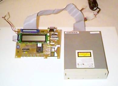
A picture of the original board is shown in Figure 1.
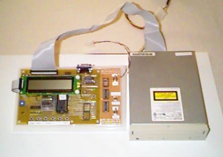
When I updated the project I returned to the original wirewrap board
and modified it. After verifying the changes I stuffed one of the original
PC boards and modified it. See Figure 2.
Project Hardware
The schematics can be downloaded here (PDF).
Sheets 1 and 2 are for the updated circuit. Sheet 3 shows what Sheet 1 would look like without the changes. Sheet 4 shows the original project circuit.
The differences between the original circuit and the updated circuit are:
1. The GP32 clock is either a 9.8304 MHz oscillator (Programming Mode) or a 32 MHz oscillator (User/Development Mode).
2. The serial port is half-duplex and comes from either PTA0 (Programming Mode) or PTE0 (User/Development Mode).
3. PTC0, PTC1, PTC3, and PTA7 are either connected to various levels (Programming Mode) or they go to where they are needed by the project (User/Development Mode).
Note that since the GP32's ports were not sufficient to do everything they have been expanded by the use of U2 (74HC374) and U3 (74HC244).
The 20x2 LCD display (Optrex DMC20261) is run in a write-only mode. This requires that a software timer be used instead of checking the LCD's ready flag. .
The extra signal in the SPI signal group (FSync) is used to provide a Frame Sync signal so it can talk to the Serial Port of an Analog Devices ADSP2181 Evaluation Board. (This is used in the Simulated AM Radio project.)
There are three switches to select the desired operating mode:
Power User/Dev or Programmer
User/Dev Mode
Off
x
x
Off
On
Programmer
x
Programmer
On
User/Dev
Dev Development
(Debugger)
On
User/Dev
User User Program
(CDROM Controller)
Project Software
The project software is divided into twelve areas.
1. Program Initialization: Initializes the Stack and the I/O Ports.
2. Program Startup: Looks at the User/Dev Switch and runs either the Standalone CDROM Controller or my Monitor program.
3. Monitor Program for using the project with P&E Microcomputer Systems Debugger.
4. CD Player.
5. Software Timing Functions: Software Wait Functions.
6. Programs for LCD: Power-Reset, write to LCD Instruction and Data
Registers,
write binary characters, convert binary to BCD, and put out messages.
7. Programs for Switches: Read and debounce the switches, and check for positive transitions.
8. Functions for the CDROM Drive.
9. Lower Level CDROM Drive Functions.
10. Functions for ISO-9660 CD Data Discs.
11. Various Test Functions for developing software for the CDROM Drive.
12. Interrupt Functions: Read the switches.
Downloadable Software
I am making software for the project available for download under the following terms.
The source code is Copyright 1999, 2001, 2003 Jed Margolin (comments@jmargolin.com).
1. Permission is granted to individuals to make copies for their own use.
All other use requires permission of the copyright holder.
2. The author is not held liable for the use of the information contained in the article and accompanying documentation.
3. The article and accompanying documentation may be freely distributed as long as:
a. Jed Margolin is given credit as the author.
b. The article and/or accompanying documentation may not be changed in any way without the copyright holder's consent.
c. No money is charged for distributing the article and/or accompanying documentation.
d. All
those receiving or distributing the article and/or accompanying documentation
agree to be bound by these terms (1 - 3).
If you agree to these terms and wish to download the code do it here.
If not, then don't.
Playing an Audio CD
The block diagram of the program used for playing an Audio CD is shown
in Figure 4. The commands for playing an Audio
CD are found in the SFF-8020i standard. I originally planned to implement
the Forward Scan and Reverse Scan commands, but none of the three CDROM
drives I tried would recognize these commands. (I tried a Mitsumi 16X and
two Mitsumi 40x drives.)
The first computer that I connected my own circuitry to was a PDP8 in
the college lab. The PDP8 was one of the original embedded computers, if
only because you needed a forklift to move it. The first computer that
I actually owned was a KIM-1 with a 6502. It allowed me to develop circuitry
for which I received my first patent. I have fifteen patents in fields
such as video game technology, graphics memory architecture, aircraft navigation
and control, and digital map data compression.